This thread has been locked.

If you have a related question, please click the "Ask a related question" button in the top right corner. The newly created question will be automatically linked to this question.

TPA3255: SE to Diff Input Stage Star Ground

Part Number: TPA3255
Other Parts Discussed in Thread: TPA3251EVM

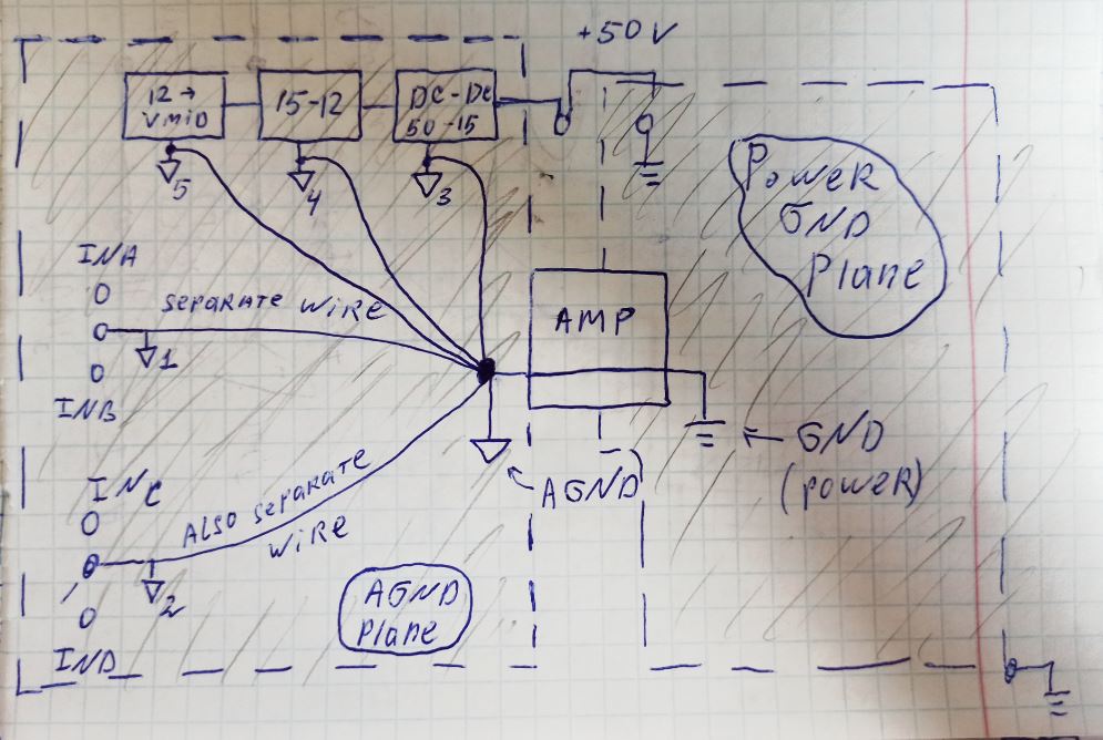
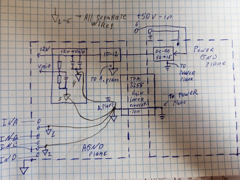
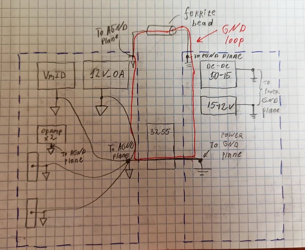
Hello. In this paper "Star" grounding configuration shows significant improvements for THD+N parameter.But as i see, TPA3255 PCB rev.A does not have this feature, however TPA3251EVM does, but only halfway (no separate AGND for 12V and VMID). I would like try to implement this technique in my own design using TPA3255 and i got following question: In paper separate grounding used not only for analog inputs but for 12v supply and VMID supply also. Does this mean, that i should ground 15V supply (wich then creats 12V) also separately to AGND or its should stay at Power GND, how can i make separate AGND for 12V supply then? I really sorry for roughness of the picture, but i hope you can better see what i mean.

  • Hi,

    I think you can keep the 15->12V power supply as PGND. And on the op-amp side, use AGND. Then connect the PGND and AGND with a ferrite bead.

    This will keep all the signal chain refer to the AGND, while the power supply related ground as PGND.

    Does it make sense for you?

    Thanks!

    Regards,

    Sam

  • Hello, Sam! Thanks for quick response. I think i got it. I has redrowed my picture to make sure i understood you correct, can you please look at it? Since we already have one connection (AGND->PGND) inside a chip itself, If i connect AGND plane and PGND plane elsewhere with a ferrite bead isn't it like crating GND loop? 

    Regards,

    Vasiliy

  • Hi,

    Single point A/PGND connection should be used to avoid GND loop, so no need to add a ferrite bead as you already have one to connect the A/PGND together.

    Thanks!

    Regards,

    Sam

  • Well thank you. Then I want to clarify for the last time whether I understood correctly. So, to achieve the best result:

    1. "50-15 V DC-DC" supply should seat at PGND plane as "15-12V" one.

    2. 12V_OA(for OPAMPs) and VMID grounds goes straight to AGND point near chip by separate wires. (Or it is enough to lead only the ground of VMID supply with a separate wire and leave 12V_ОА anywhere on the AGND?)

    3. All input's AGND shoul go with separate wires to AGND point near chip and OPAMP's AGND can pe placed anywhere at AGND plane due opamp high PSRR.

    4. Inner connection inside TPA3255 from AGND pins (12, 13) to PGND pins (25, 26, 33, 34, 41, 42) is necessary and sufficient for connect AGND to PGND at whole PCB.

    Regards,

    Vasiliy

  • Hi Vasiliy,

    Regarding 2, I think it is enough to lead only the ground of VMID supply.

    Regarding 4, please make sure a 0R resistor or ferrite bead connection is used between AGND and PGND on PCB.

    Thanks!

    Regards,

    Sam

  • Hello, Sam! I apologize for my meticulousness, and I hope I do not take much of your time. I got your point regarding 2, but I am at a loss about 4. Are pins 12, 13 and 25, 26, 33, 34, 41, 42 not connected inside the TPA3255 chip?

    My idea is to connect AGND plane and PGND plane directly through the chip, as shown in the picture. At lefthand side of PCB I have separate AGND plane and at the righthand side I have separate PGND plane. There is no connection between two planes until I place TPA3255 at PCB. At lefthand side of TPA3255 we have AGND pins 12 and 13 and at righthand side we have PGND pins (25, 26, 33, 34, 41, 42). So, placing chip at its location connects AGND and PGND planes together through the chip at ONE location. If these contacts are already connected inside the chip, then no additional connections can be made so as not to create an GND loop (as in the figure above). Or are these contacts not connected inside the TPA3255? Could you give a little more detailed comment on this question, please?

    Regards,

    Vasiliy

  • Hi Vasiliy,

    Actually the AGND (on the left bank) is not connected to the PGND (on the right bank) inside the device.

    So please use a ferrite bead or 0R resistor to connect them together on your PCB.

    Thanks!

    Regards,

    Sam

  • God bless TI! Thank you Sam! You helped me a lot, thanks for the technical support! Good luck to you!

    Regards,

    Vasiliy