This thread has been locked.

If you have a related question, please click the "Ask a related question" button in the top right corner. The newly created question will be automatically linked to this question.

TLV320AIC3101: DOUT

Part Number: TLV320AIC3101

Hi,

My customer is evaluating the TLV320AIC3101.

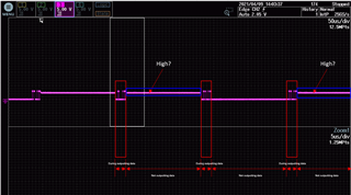
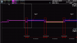
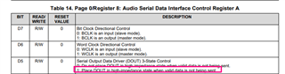
They set "1" into the register 8 D5 bit and DOUT is pulled down via a resister. 

However, DOUT outputs as below High during valid data is not being sent.

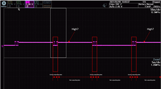
Is this correct behavior?  

Best Regards,

Kuramochi

  • HI Kuramochi-san,

    This looks to be correct behavior. The DOUT level will follow the level of the last bit transmitted. For example, on DOUT, if the last bit sent is a "1", DOUT will remain HIGH when no data is transmitted. If the last bit sent is a "0", DOUT will remain LOW when no data is transmitted. Let me know if this is not clear. 


    Regards,

    Aaron Estrada

  • Aaron-san,

    Thank you for your reply.

    It is mentioned that "when valid data is not being sent" on Register 8 D5 bit.

    Does it mean that "when valid data is not being sent" is not included in the above waveform?

    Best Regards,

    Kuramochi

  • Hi Kuramochi-san,

    Valid data is when the device is sending the configured number of bits. If set to 16-bit data, after 16 bits, there is no data and you can see this in your image above. Configuring the device this way is used for TDM mode. When one device is done sending data, it will be set to a high impedance state and the output will latch high or low so the other devices on the bus can send data. 

    Regards,

    Aaron Estrada

  • Hi Aaron-san,

    Thank you for your help.

    I'm confused.

    I think that the inside of blue rectangles terms are "when valid data is not being sent".

    However, the output is high nevertheless the DOUT is pulled down.

    Why is DOUT high during this period?

    Please let me know if I misunderstand.

    Best Regards,

    Kuramochi

  • Hi Kuramochi-san,

    You are correct in that the blue rectangle in the image signify that valid data is not being sent. When this is the case, the device goes into a high impedance state and will hold DOUT either HIGH or LOW depending on the last bit being transmitted. There is no reason to pull DOUT low. 

    Regards,
    Aaron Estrada

  • Hi Aaron-san,

    Thank you for your help.

    I have additional questions.

    1. 

    In the blue rectangle, the DOUT node is not low nevertheless the DOUT node is pulled down by the external resistor.

    Does it mean that anything(except for DOUT pin of TLV320AIC1301) is pulled up this node?

    2.

    Do you think that valid data is not being sent during the following the yellow rectangle?

    If yes, why do two states exist as the blue rectangle and the yellow rectangle?

    Best Regards,

    Kuramochi

  • Hi Kuramochi-san,

    1. I am not sure about the internal architecture for holding the line high but the device will hold DOUT high when the last bit transmitted is HIGH. 

    2. Yes, the yellow rectangle also shows when valid data is not sent. As I stated in a previous reply, the two states exist because the device will hold DOUT at the same level of the last bit transmitted. You can see that right before the blue rectangle, the last bit transmitted was a "1" so the device will hold DOUT high. Before the yellow rectangle, the last bit transmitted was a "0" so the device held the line LOW. 

    Regards,

    Aaron Estrada

  • Hi Aaron-san,

    Thank you for your help.

    How much is the resistance of the High impedance state?

    Best Regards,

    Kuramochi

  • Hi,

    How is this situation?

    Best Regards,

    Kuramochi

  • Hi Kuramochi-san,

    Apologies for the delay on this question. The post was previously marked as "Resolved" so the thread was closed. 

    I believe there to be a tristate buffer on the digital interface pins that are used to place those pins in a Hi-Z state. I will need to confirm. 

    Regards,

    Aaron Estrada