Other Parts Discussed in Thread: CLOCKPRO
Hi,
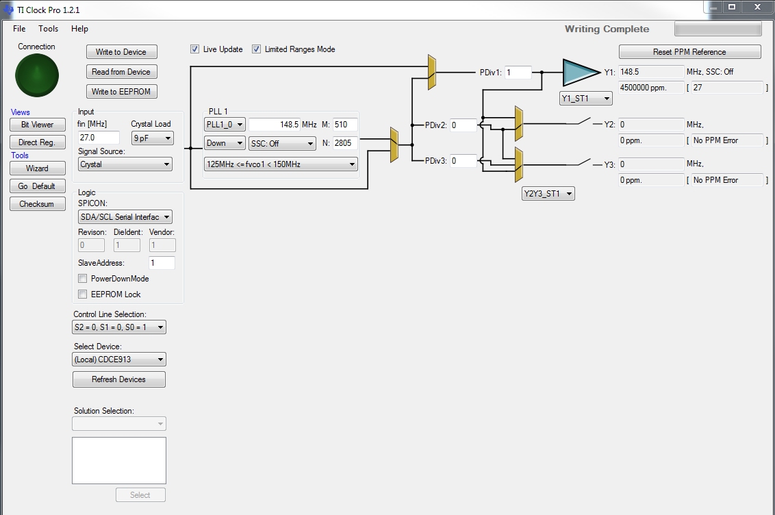
I am now trying to configuring the CDCEL913 to output the specified clock frequency on the Y1, Y2, and Y3 output.
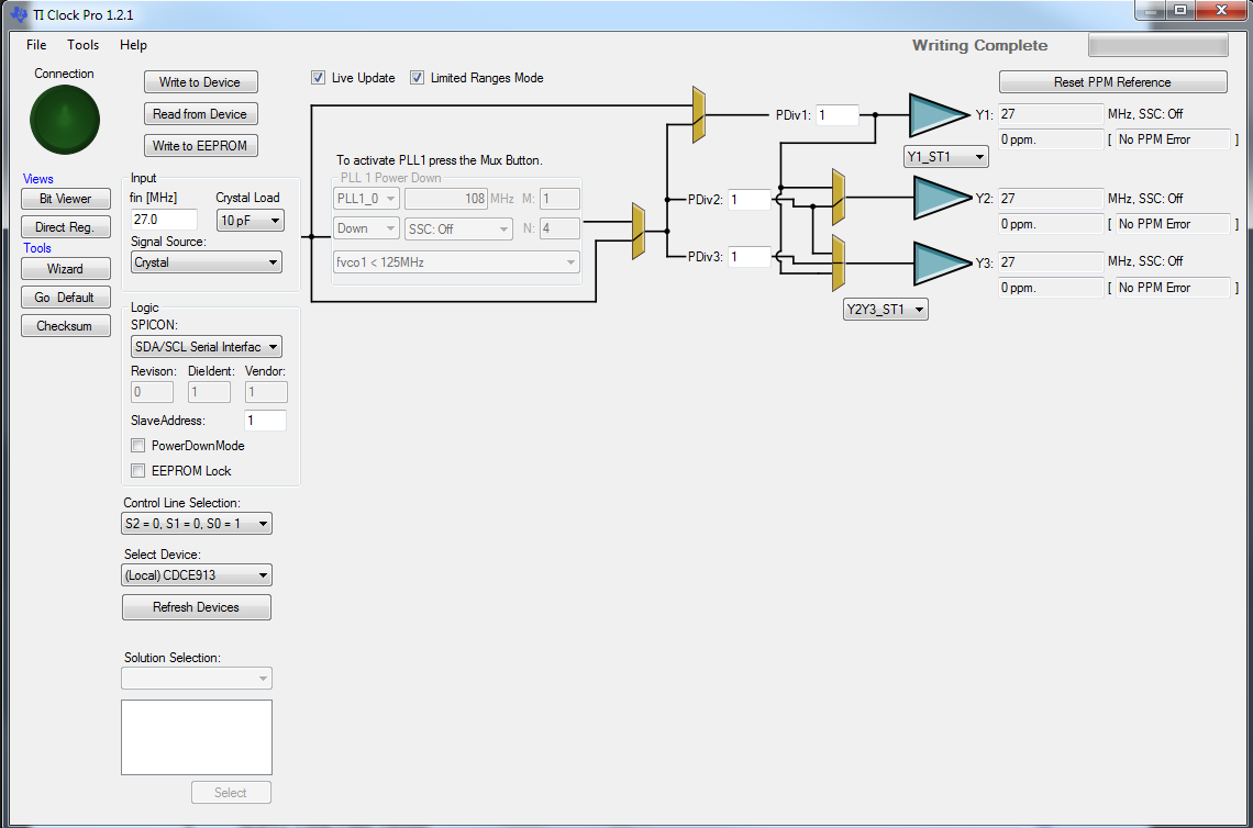
By checking the data sheet, the chip will output 27MHz frequency on Y1 ~ Y3 by default if the input clock source is 27MHz after the S0 input is set to 1. I do measure the 27MHz output on the scope after setting S0 to 1. However, none of the clock output on Y2 and Y3 if I write back the register values read from CDCEL913.
Following are my test procedures by running a small application on the device.
1. Set S0 to 1.
2. Read back the registers(register address, value) through the I2C bus using byte mode(bit7=1 | reg address).
{0x02, 0xB4},
{0x03, 0x01},
{0x04, 0x02},
{0x05, 0x48},
{0x06, 0x60},
{0x10, 0x00},
{0x11, 0x00},
{0x12, 0x00},
{0x13, 0x00},
{0x14, 0x45},
{0x15, 0x02},
{0x16, 0x00},
{0x17, 0x00},
{0x18, 0xAF},
{0x19, 0x50},
{0x1A, 0x02},
{0x1B, 0xC9},
{0x1C, 0x00},
{0x1D, 0x40},
{0x1E, 0x02},
{0x1F, 0x08}
3. Write back these registers with the same values listed above and measure the Y2/Y3 output.
Is there anything wrong of my testing procedures? Should I set S0 to 1 after the write register operation? Or there is any special rules for the write register operation?
Thanks.
Todd