This thread has been locked.

If you have a related question, please click the "Ask a related question" button in the top right corner. The newly created question will be automatically linked to this question.

LMK00308: LMK00304/08 bias voltage

Part Number: LMK00308
Other Parts Discussed in Thread: LMK00304,

Hi All,

I am sending this email to ask some questions on input bias voltage and termination resistor of LMK00304/08.

My customer has applied LMK00304 and LMK00308 to new system and they are used for LVDS interface.

Customer said that the datasheet recommends to place the termination resistor before the AC coupling cap.

However, they found that the input bias voltage on both inputs is different when they measured the waveforms of LMK00308 input. After changing the placement of termination resistor to behind AC coupling cap, the bias voltage became same on both inputs. Please find the attached to see the scope captures.

 Regarding the placement of termination resistor, they have some questions.

Please refer to below comments, would you answer those questions?

  •  Why do both inputs have the different bias voltage when the termination resistor is placed before AC coupling? Could the output pins supply the normal waveform even if there is the difference on bias voltage?
  • Looking at the attached file, both inputs could have same bias voltage after changing the placement of termination resistor behind AC coupling cap. Could the termination resistor be placed following AC coupling as customer modified? Please let me know if you have any concern on this placement.
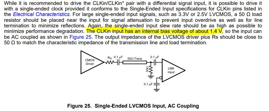
  • The datasheet states that the CLKin input has an internal bias voltage of about 1.4 V but you can see the bias voltage is 1.2V from the scope capture when placing the termination resistor behind AC coupling cap. Could you let me know why input bias is fixed as 1.2V not 1.4V?

 LMK00304 terminated resistor_040319.pptx

Thanks in advance.

Best regards,

Sammy

  • Hi Saemyi,

    The correct connection is to have the termination resistor before the AC coupling cap.
    The unbalanced input bias voltage is intentionally added so that when there is no input clock, the output of the clock buffer is quietly staying at either HIGH or LOW (usually LOW). This is called failsafe. Without failsafe, the output may be toggling between HIGH and LOW.
    The absolute bias voltage of the P and N pins are not very important, usually they are differ by 200mV, which is a magic number that most of the differential buffers can distinguish between 1 and 0.

    Since the output from LMK00304 is LVDS, DC-couple is recommended. So the termination resistor should be placed before the AC caps.
  • Hi Noel,

    Thanks for fast response.

    My customer has more questions on your answer. Please refer to below questions, would you please provide your answers?

    1) The reason why customer uses AC coupling, the datasheet shows that there are different bias voltage on input and output.

    Looking at the datasheet of page 10 of LMK00304, the output offset voltage is 1.25V while the input bias voltage of LMK00308 is about 1.4V.

    Since the bias voltage between the output LMK00304 and the input of LMK00308 is different, they applied AC coupling between both devices.

    Despite the bias voltage difference between the output LMK00304 and the input of LMK00308, could they use DC-couple between LMK00308 and LMK00304 instead of AC coupling without any issue?

    You recommended to use DC-couples but also recommended to place the termination resistor before the AC caps. Would you explain what it meant?

    2) When Samsung placed the termination resistor behind AC coupling capacitor, the bias voltage became 1.2V not 1.4V. Would you explain why the input voltage of LMK00308 has 1.2V bias voltage in this case? 

    3) Customer is concerned about the internal failsafe, which input P and input N have the different bias voltage. They think it could cause the duty cycle of clock to be changed. Would you confirm that internal failsafe function doesn't have impact on the output clock performance?

    Thanks.

    Best regards,
    Sammy

  • Hi Sammy,

    I checked the spec again, since the input common mode voltage of LMK00308 is between 0.25V to Vcc-1.1V, if the input signal is LVDS, you are free to select either DC- or AC-coupling. That is:

    LVDS is a standardized interface (TIA-EIA-644), the output offset voltage, Vos is standardized to approx. 1.25V.

    LVDS is a current source. As such, the simplest and best interconnection is DC-couple to a 100 ohm termination. 

    If we put a small resistor between P and N, there will be some current flowing between these pins and as a result, their bias voltages are alternated.

    In the above diagram, if we keep the capacitors, then the left hand side is a perfect match to a LVDS driver. The right hand is also a perfect match to the LMK00308 input as the internal bias voltage can be kept unchanged - the failsafe characteristic is maintained. 

    Remember the output of a differential driver will be equal to 1 if V+ is greater than V-. Output will be equal to 0 if V- is greater than V+. So the failsafe will not change the duty cycle, in fact, failsafe is irrelevant to duty cycle.