This thread has been locked.

If you have a related question, please click the "Ask a related question" button in the top right corner. The newly created question will be automatically linked to this question.

LMK04208: LMK04208

Part Number: LMK04208

Hi

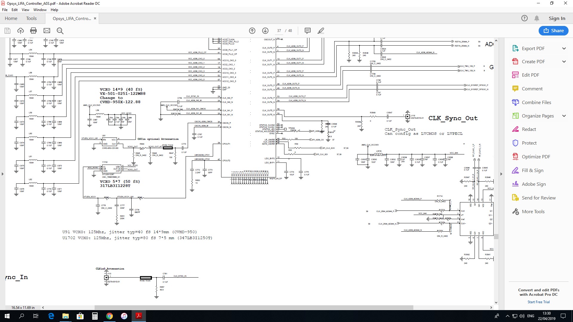
At our design we use LMK04208 to drive Xillinx FPGA in similear design as LMK04208 eval with external VCXO . We are using two similar cards when the first card is master which run as stand along mode with the below config file, and second card as slave where the master 125Mhz sync clock drive the slave clk_in_0 input.

We got 4 running card which each of them can act as slave (where it lock to the master 125Mhz clock) but one of the 4 cards fail to push (as master) the other 3 cards!!!

When looking with 20Ghz scoop on the LMK04208 output we almost dont see any differences

Do you got any idea what can cause this issue?

How can we inspect the jitter output of  LMK04208??

The master config (where for slave config we change only input from clk_in_1 input to clk_in_0 input)  : 

R0 (INIT) 0x00160040
R0 0x00140300
R1 0x00140301
R2 0x00140062
R3 0x80140603
R4 0x00140304
R5 0x80140185
R6 0x01100006
R7 0x01300007
R8 0x04010008
R9 0x55555549
R10 0x9102410A
R11 0x0401100B
R12 0x1B0C006C
R13 0x2302826D
R14 0x0200000E
R15 0x8000800F
R16 0xC1550410
R24 0x00000058
R25 0x02C9C419
R26 0xAFA8001A
R27 0x10001E1B
R28 0x00201E1C
R29 0x0180019D
R30 0x0200019E
R31 0x003F001F

Thanks

Oded

  • Hello,

    Let me be sure I understand the situation..

    You have built 4 cards. Each card can be master or slave.
    All 4 cards work as slave.
    3 cards work as master, but one card does not work as slave.

    Can you clarify more what you mean by, "but one of the 4 cards fail to push (as master) the other 3 cards!!!"
    - Does the card not lock as master?
    - Is there an output from the master?
    - Does the slave lock?
    - Without understanding better the failure, I'm limited in my ability to help.

    So the attached waveform shows 125 MHz. Is this from the card not working as master? Does a non-working card produce any output?
    - I don't expect and possible jitter issue as the reason for failure. Even with jitter devices should lock.

    ---

    To debug a PLL not locking, I suggest looking at the PLL# R/2 and PLL# N/2 at the same time using LD_MUX and HOLDOVER_MUX. What you should see is a frequency at half the phase detector rate line up between the two devices. If a clock is missing or the wrong frequency this can give a clue as to what is not working. This can be done for PLL1 and PLL2.

    73,
    Timothy
  • Dear Timothy,

    Even for us it hard to understand the issue where master card with good output signal ccause others card not to lock?

    We have built 4 cards which each card have one LMK with Single ended output and single ended input that used to sync 2 cards. One card can define as master or slave, where master mode include the attach config and slave mode include one change where we define input clk_in_0 

    So the master act is free run card, and the slave should lock to the output of the master and sync the clock

    This issue work with one exception: one card (#1) of the four will cause the other 3 cards (#2-#4)  that act as slave not to be lock. all other setup, where the 3 cards (#2-#4) act as master to other cards is working well. The card (#1) that dont lock other cards is working fine as slave

    When we looked on the master output of card #1 or cards#2-4 we couldn't see any diff in the signal (the image send at previous post. the same go with looking on the slave input clk_in_0 pin

    It indeed strange issue that master card with good eye output do not cause all other slave cards not to lock??

    About your question: 

     Does the card not lock as master? The slave not lock to one master of the 4 cards 
    - Is there an output from the master? Yes Output 5 
    - Does the slave lock? Not lock with one master (Card #1) all other master couse slave to lock

    To debug a PLL not locking, I suggest looking at the PLL# R/2 and PLL# N/2 at the same time using LD_MUX and HOLDOVER_MUX. What you should see is a frequency at half the phase detector rate line up between the two devices. If a clock is missing or the wrong frequency this can give a clue as to what is not working. This can be done for PLL1 and PLL2.

    We have compare the testpoint with master #1 -> slave #4 and master #2->slave #4

     master #2->slave #4: Pll1_N - Lock clock, PLL1_R - Lock clock

                                      Pll2_N - Lock clock, PLL2_R - Lock clock


    master #1->slave #4: Pll1_N - Lock clock, PLL1_R - not Lock clock!

                                      Pll2_N - DC 3.3V , PLL2_R - DC 0 V


    Master config:

    R0 (INIT) 0x00160040
    R0 0x00140300
    R1 0x00140301
    R2 0x00140062
    R3 0x80140603
    R4 0x00140304
    R5 0x80140185
    R6 0x01100006
    R7 0x01300007
    R8 0x04010008
    R9 0x55555549
    R10 0x9102410A
    R11 0x0401100B
    R12 0x1B0C006C
    R13 0x2302826D
    R14 0x0200000E
    R15 0x8000800F
    R16 0xC1550410
    R24 0x00000058
    R25 0x02C9C419
    R26 0xAFA8001A
    R27 0x10001E1B
    R28 0x00201E1C
    R29 0x0180019D
    R30 0x0200019E
    R31 0x003F001F

    Thanks

    Oded


  • Dear Timothy or Other LMK TI member,

    Can you please replay is issue

    thanks

    Oded

  • Hello Oded,

    Sorry for the delay...

    Oded Globerman said:
    So the master act is free run card, and the slave should lock to the output of the master and sync the clock

    To confirm.  So the board has CLKin0 as an input to PLL1, PLL1 does jitter cleaning with a VCXO, and PLL2 is used to generate your outputs.

    * When you say free run for master mode, you mean there is no clock applied to CLKin0?  This means the user case is more like single loop PLL2 and that PLL1 will rail.  This could be the reason why you are getting device to fail locking to board #4.

    I notice you have three different VCXOs listed. Which one are you using?  Are you using the same one on all boards?

      - VX-501-0251-122M88
      - CVHD-950-125.000
      - 317LB3I1228T

    It is possible that when the master rails, it rails to a frequency higher or lower than the other VCXOs can tune....  Then the slave will not be able to lock.  VCXOs have a relatively narrow locking range. 

      * Try providing a 125 MHz clock from a signal generator to the master to see if that helps.

      * Alternatively, you could put the device into holdover mode with the Vtune forced to Vcc / 2.  You could achieve this by programming R15 as 0x8010802F.

    73,
    Timothy

  • Hi Timothy

    thanks for the reply

    answering you question 

    So the master act is free run card, and the slave should lock to the output of the master and sync the clock   -  Yes

    To confirm.  So the board has CLKin0 as an input to PLL1, PLL1 does jitter cleaning with a VCXO, and PLL2 is used to generate your outputs. -

    OG-Yes

     When you say free run for master mode, you mean there is no clock applied to CLKin0?  -

    OG-yes, The master card define the phase and clock

    I notice you have three different VCXOs listed. Which one are you using? - 

    OG-CVHD-950-125.000 in master and slave cards

    It is possible that when the master rails, it rails to a frequency higher or lower than the other VCXOs can tune. -

    OG-When connecting 20ghz scope we got the same figure in master #1(that slave do not lock with)   and master #2 (image in may 30). We indeed look on this as issue #1 and We even try to replace the VCXO between Card #1 and Card #2, Card #1 still didnt lock slave card (maybe we should return on this test?, maybe we had some confusion in this test??)

    Do you got any other test idea that could help us understand better the issue?

    Thanks

    Oded

  • You would not be able to measure the frequency to the accuracy you need with the scope.  For CVHD-950 the frequency pulling APR min is +/- 20 ppm.  So if for example you had a +/- 50 ppm signal as reference, the VCXO may not be able to tune to the extremes of the +.- 50 ppm to lock.

    Can you use a frequency counter to measure the OUT5 frequency of all 4 boards in free run/master mode?

    I suggest providing a frequency accurate signal to CLKin0 for master or programming R15 as 0x8010802F to enable holdover and force the Vtune to Vcc/2 to keep frequency of master as accurate as possible by open loop.

    73,
    Timothy

  • Dear Timothy,

    Thanks to your support we found the root of the problem. Indeed when connecting freq counter we found that working master is -50 to -60ppm shift (124.9930mhz) while non locking master is about -70ppm (124.9919mhz) freq shift

    We looked on the VCPOUT1 and found it around 0V. So the main problem is that PLL 1 is not loop the VCXO and pushing it the the lower edge! (With high speed scope we were blind to find this). 

    So , does it mean our config file have some error?

    The original LMK config  was design to work with  122.88Mhz VCXO, We have replace and adjust it to work with 125mhz vcxo.

    Have we missed some thing in the config that cause PLL1 not to function. Attach again our config file?

    R0 (INIT) 0x00160040
    R0 0x00140300
    R1 0x00140301
    R2 0x00140062
    R3 0x80140603
    R4 0x00140304
    R5 0x80140185
    R6 0x01100006
    R7 0x01300007
    R8 0x04010008
    R9 0x55555549
    R10 0x9102410A
    R11 0x0401100B
    R12 0x1B0C006C
    R13 0x2302826D
    R14 0x0200000E
    R15 0x8000800F
    R16 0xC1550410
    R24 0x00000058
    R25 0x02C9C419
    R26 0xAFA8001A
    R27 0x10001E1B
    R28 0x00201E1C
    R29 0x0180019D
    R30 0x0200019E
    R31 0x003F001F

    Timothy, Thanks again for target us on the problem

    Thanks

    Oded


  • Hello Oded,

    Change R15 to 0x8010802F in the master.  This will force holdover (FORCED_HOLDVER = 1) and therefore cause PLL1 to force a Vtune of Vcc/2 (MAN_DAC=512, and EN_MAN_DAC=1) volts on the VCXO.  This should raise the voltage and therefore the frequency of the VCXO to closer to 0 ppm.  If not sufficient, please try increasing MAN_DAC to a higher value.  You should be able to measure the impact of changing MAN_DAC by seeing Vtune1 of master change and therefore output frequency of master change.  Then, as slave attempts to lock, you should see a valid VCXO voltage on the slave instead of 0 V.

    I don't recommend the same configuration for master and slave.  Master should not free-run PLL1, it should force holdover.

    73,
    Timothy

  • Dear Timothy,

    Thank you for the replay. We indeed change the master card to holdover mode and that force the VCXO to VCC/2.

    The issue that we dont understand is does the LMK allow dynamic VCXO tracking that will follow the VCXO to 125Mhz?

    At hold over stage the VCXO is force for fix DC value?

    Does the master card should work in double mode PLL as today or at single PLL mode (DS page 46)?

    Which setup will give us the best stable freq close to 125Mhz?

    Thanks

    Oded 

  • Hello Oded,

    Oded Globerman said:
    The issue that we dont understand is does the LMK allow dynamic VCXO tracking that will follow the VCXO to 125Mhz?

    When in holdover, PLL1 is operating in open loop.  You could tweak the VCXO to 125 MHz by adjusting the MAN_DAC value which will result in a different VCXO voltage applied.  But vs. temperature, voltage, etc - there could be some drift in frequency.  Only by providing a valid reference to PLL1 master could you lock to 125 MHz in a closed loop fashion.

    Oded Globerman said:
    At hold over stage the VCXO is force for fix DC value?

    Yes, but you can change it by programming MAN_DAC register.

    Oded Globerman said:
    Does the master card should work in double mode PLL as today or at single PLL mode (DS page 46)?

    It could work in either dual loop mode or single loop mode.  If you used an XO instead of VCXO for master, then single loop mode.  If using VCXO, this assumes you are providing a reference to PLL1.  Dual loop mode is good for obtaining best performance in the following two cases:

      (1) jitter cleaning -- if your reference is noisy (like a recovered clock) it will achieve jitter cleaning through a narrow loop bandwidth of PLL1.

      (2) best reference for PLL2 - if your reference is low frequency (like 10 MHz), you can get better PLL2 performance by providing a higher reference frequency, like >= 100 MHz.  By using 10 MHz to PLL1 reference, then 125 MHz to PLL2 reference, optimum phase noise / jitter performance is achieved.

    Either dual loop or single loop setup will give you a stable frequency close to 125 MHz to the ppm error of your reference.  You are currently running your master WITHOUT a reference.  By setting VCXO to Vcc/2, you are improving your reference accuracy.  But I expect it will not be as good as an XO.

    73,
    Timothy