This thread has been locked.

If you have a related question, please click the "Ask a related question" button in the top right corner. The newly created question will be automatically linked to this question.

LMK05028: Questions for 2-Loop TCXO-DPLL Mode

Part Number: LMK05028

Hello, Team,

My customer is tring to use DCO mode of LMK05028. The costomer would like to use DCO without clock. We have a few questions for 2-loop TCXO-DPLL mode.

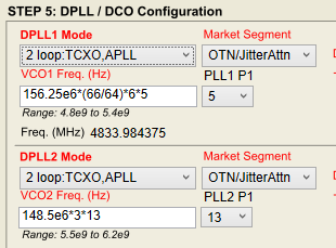
1. Could you review the below configuration? Please let me know if there is any concerns.
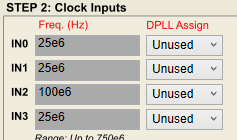

There is "Run cancelled. DPLL[1,2] missing input assignment" error for this configuration.

2. The customer would like not to use IN0~3 DPLL assign, but there is error message “DPLL[1,2] missing input assignment” Is it possible not to use IN0~3?

3. An error occurs when PLL1 and PLL2 are interchanged. When CH0-3 is assigned to PLL1 and CH4-6 is assigned to PLL2, there is error message “OUT [4: 7] bank need 1+ clock from PLL1”. What is this error?

I will send the TCS file, if you need.

Best Regards
Satoshi Yone

  • Hello Yone-san,

    I've contacted the appropriate applications engineer, and he should be able to respond to this in a few hours.

    Regards,

  • Hello,

    Satoshi Yone said:
    1. Could you review the below configuration? Please let me know if there is any concerns.

    I don't see an issue from this limited info... See item #2 for my comment on There is "Run cancelled. DPLL[1,2] missing input assignment" error for this configuration."

    Satoshi Yone said:
    2. The customer would like not to use IN0~3 DPLL assign, but there is error message “DPLL[1,2] missing input assignment” Is it possible not to use IN0~3?

    The software is wanting to calculate the DPLL information and it can't since you haven't given it any inputs.  It is possible to use the device without an input.  It will operate in a holdover state.  However the script is still wanting to calculate DPLL values.  So just enable one of the inputs as reference to DPLL1 and 2.  Then when it is not present it will be detected and operate in holdover as the reference validation will fail.  You can enable the frequency detect threshold and the missing clock detector.

    Satoshi Yone said:
    3. An error occurs when PLL1 and PLL2 are interchanged. When CH0-3 is assigned to PLL1 and CH4-6 is assigned to PLL2, there is error message “OUT [4: 7] bank need 1+ clock from PLL1”. What is this error?

    I expect this is due to some internal pre-driver configuration requiremenet.  The datasheet calls this out in section 6 for pin functions and in the detailed design procedure, section 10.2.2 in step #5, so it makes sense that the GUI is warning you/preventing you from breaking this rule  Note you wouldn't want to swap the outputs anyway as optimum spur performance is achieved with PLL1 driving OUT[4:7] and PLL2 driving OUT[0:3].

    73,
    Timothy

  • Hi, Timothy,

    Thanks for your support. I will post a new thread.

    Best Regards,
    Satoshi Yone