This thread has been locked.

If you have a related question, please click the "Ask a related question" button in the top right corner. The newly created question will be automatically linked to this question.

LMK04832: Unable retrieved phase noise results for LMK04832

Part Number: LMK04832

Hi,

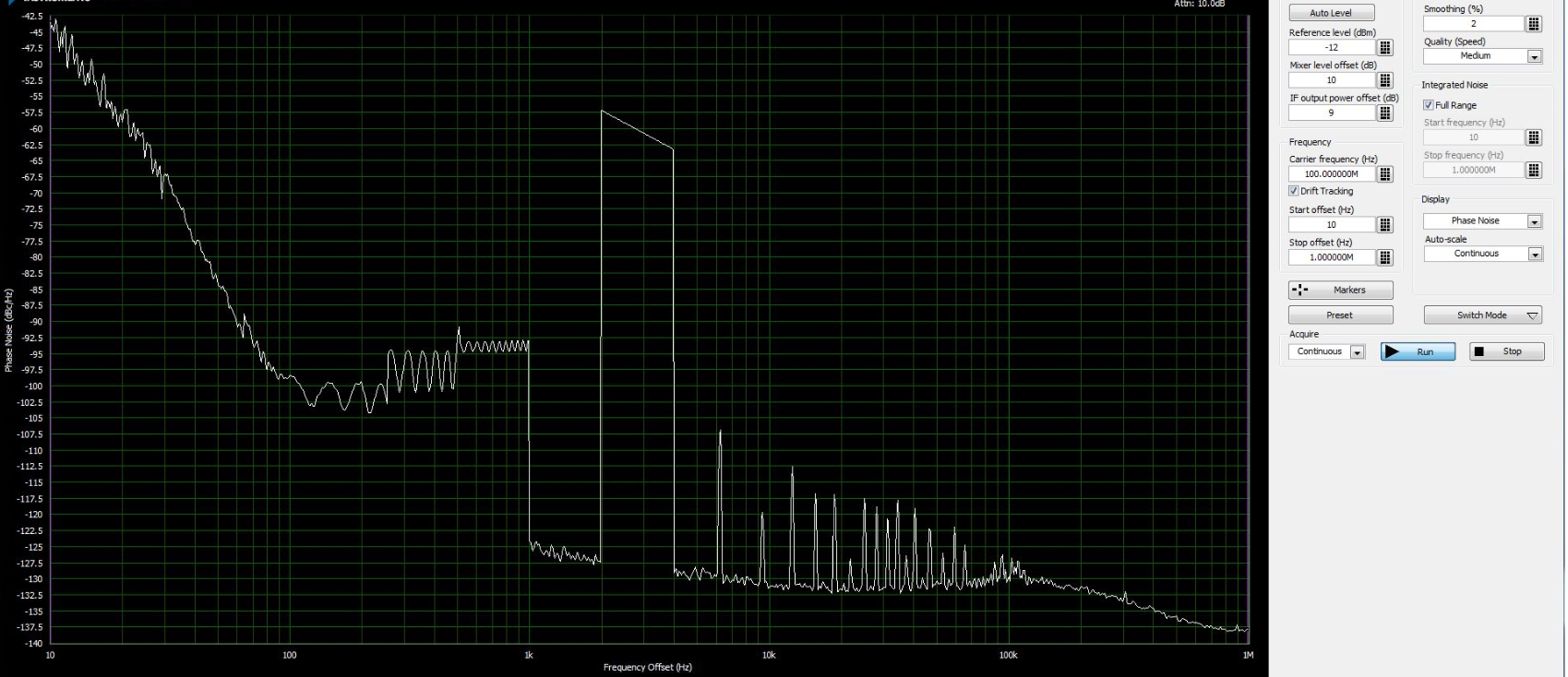
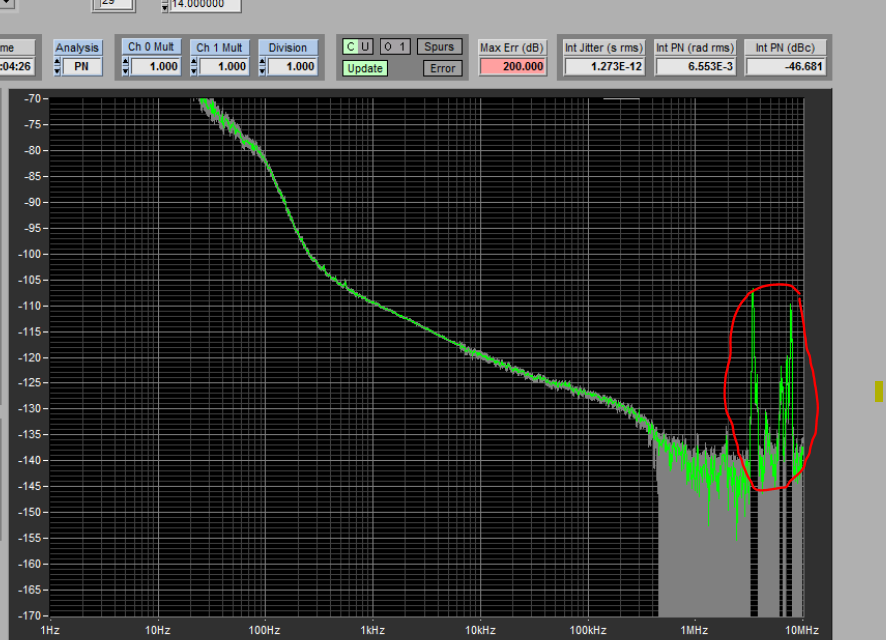
I having difficulty to understand why my phase noise measurement retrieved is weird. In the design, we have added LEDs at Status_LD1 and Status_LD2 to check whether the PLL locked. For my understanding, once saw PLL locked mean the system is stable. So we try to carry phase noise measurement, unfortunately the results is not expected. I never see this kind of waveform appear in my LMK04832EVM board. We also simulate the loop filter using TI Platinum Pro to see the waveform but we unable retrieved this kind of waveform. The simulation shows the system is stable. For my testing, I required to solder additional SMA connectors on the CLKOUT(100MHz) of LMK04832 so that we can plug into the test setup. Besides that, the test board doesn't have any shield to prevent noise coupling into it. Does anyone have any idea about this? Is it my setup not so appropriate that effect the results?

  • Hello,

    Can you confirm you are using the EVM or your own PCB design for the plot above.

    What is the reference?  Can you post your configuration?

    73,
    Timothy

  • Hi,

    Sorry for late reply, the setup is tested on our own design board and the issue has been solved. It was due to the program is keep looping instead of running once only. But now we have another issue where there is spur at ~3MHz and ~7MHz offset in the result when we didnt placed 0.1uF bypass capacitor in series to the receiver side. The spur doesnt occur when there is 0.1uF capacitor there. However for our design, we cannot placed a bypass capacitor on that as we need the LVDS has a positive offset voltage to deliver into a FPGA module that only support positive voltage signal. For my understanding, LVDS signal not necessary need a bypass capacitor, is there anyway to remove the spur without adding the bypass capacitor or any suggestion to improve the results? I have attached the setup and result as shown below. Thanks.

  • Ee Wen Quek said:
    For my understanding, LVDS signal not necessary need a bypass capacitor,


    You are correct, LVDS doesn't require a bypass capacitor.

    Ee Wen Quek said:
    But now we have another issue where there is spur at ~3MHz and ~7MHz offset in the result when we didnt placed 0.1uF bypass capacitor in series to the receiver side. The spur doesnt occur when there is 0.1uF capacitor there. However for our design, we cannot placed a bypass capacitor on that as we need the LVDS has a positive offset voltage to deliver into a FPGA module that only support positive voltage signal.

    On which channel does the spur occur?  Is it on both channels at the same offsets?

    What sort of bypassing do you have on the supply of Vcc4_CG2 (CLKout6) and Vcc11_CG3 (CLKout8).

    Ee Wen Quek said:
    is there anyway to remove the spur without adding the bypass capacitor or any suggestion to improve the results? I have attached the setup and result as shown below. Thanks.

    Can you advise how you made these measurements?

    73,
    Timothy

  • Hi,

    1. On which channel does the spur occur?  Is it on both channels at the same offsets? 
      Both channels get the same results at same offset.
    2. What sort of bypassing do you have on the supply of Vcc4_CG2 (CLKout6) and Vcc11_CG3 (CLKout8)?
      For my design, both VCCs have 10uF, 1uF and 0.1uF parallel. Actually I have tested the evaluation board by removing the bypass capacitor at CLKOUT8, I get the spur at same offset as well. Is this something expected?
    3. Can you advise how you made these measurements?
      I am an internal spectrum analyzer that able perform phase noise test as well. Each time only one signal is taken while another side will be terminated. 

  • Hello,

    1) Can you advise how the spurs change or stay the same if you generate output frequency from VCO1 using 2949.12 MHz?  I suggest /3 for 983.04 MHz and /24 for 122.88 MHz.

    2) Do you have any input signals on pin 6 (SYNC) or 5 (RESET/GPO)?

    - Are you able to disconnect these?  If not place filter capacitor on them?

    73,
    Timothy