This thread has been locked.

If you have a related question, please click the "Ask a related question" button in the top right corner. The newly created question will be automatically linked to this question.

LMK61E07: Fractiional frequency setting problems - too low tuning range of LMK61xxx devices

Part Number: LMK61E07
Other Parts Discussed in Thread: CDCE6214-Q1, LMK03318, LMK03328, USB2ANY, LMK61E2,

Hi,

after a long fight and experiments we have not succeeded in making LMK61Exx work in the fractional tuning mode. We would like to use it in the fractional mode as a ultra-low jitter, high-frequency audio clock but it does not work as we expect reading datasheet.
Moreover, we checked with two different pieces LMK61E07-SIAT and LMK61E2BBA (125 MHz part) and not only do they not work as in DS but also each behaves differently (!). 
The E2 starts in the INTEGER mode and after setting it to the fractional mode its frequency can be fractionally adjusted up to NUM\DEN = 0.5 (but not at least 1.0 as we would expect). A change of  NDIV from 50 to 51 results in frequency of 126.3MHz instead of 127.5MHz, i.e. approx. half the expexted step. When NUM/DEN gets more than 0.5 the tuning stops.

The E7 part when powered up at default 70,67 MHz can be fractionally tuned higher (so starts in the fractional mode) up to NUM\DEN = 1.0. However, if the INT is changed more than 2% then output frequency stops reacting to tuning at all.


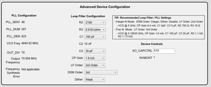
Generally, based on the datasheet we would expect tuning to +/-10%, since VCO starts at approximetly 5.0GHz and have the tuning range 5.1 +/- 0.5GHz (with equals +/-10%).

We would like to ask first how the INT + NUM\DEN tuning works in general. We would expect that INT should allow to tune within the VCO range = 4.6...5.6 GHz, even if that would generate glitches.


Second question is about NUM\DEN, could it take values greater than 1.0?


And the third question can you please provide hints what we should change in the registers so that it would allow full use of fractional mode at all frequencies ?

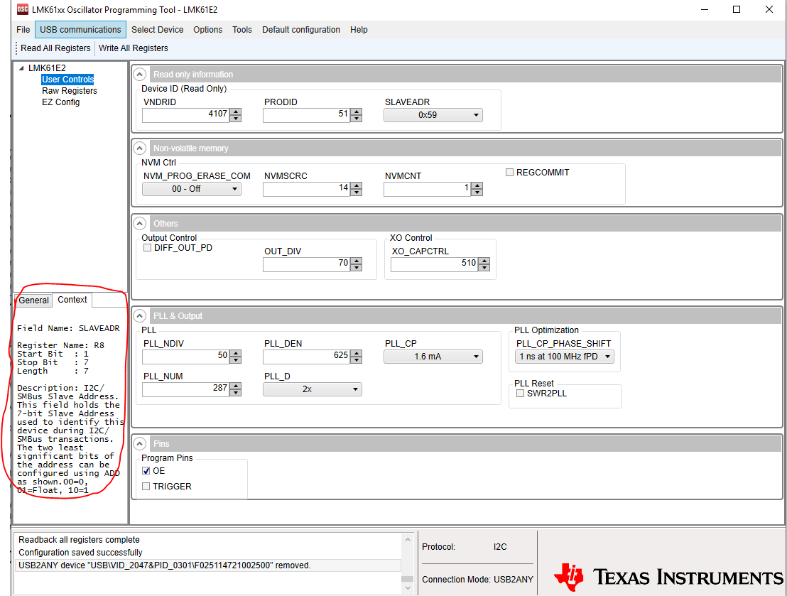
For convenience we scanned all the register values for the E07 part (as set at default) which allows to tune from it's default values up and down, but it does not work when the INT is changed by more than 1-2% (e.g. if the original R26 value (49) is changed to 52, it works only if we change values to 48, 50 or 51).

R0: 16

R1: 11

R2: 51

R3: 3

R4: 137

R5: 133

R6: 140

R7: 0

R8: 178

R9: 0

R10: 1

R11: 0

R12: 66

R13: 163

R14: 32

R15: 5

R16: 2

R17: 127

R18: 0

R19: 25

R20: 0

R21: 2

R22: 0

R23: 70

The source of clocking is a quite critical part of our high-end class D amplifier product therefore we have asked detailed questions and would like to be aware how to achieve best possible phase noise performance.

And we would like to make sure if it is actually the best part in TI offer to meet our highest requirements for high-frequency (approx. 400MHz) master audio clock that we intend to synchronize (using custom control logic) to the incoming audio clock. We would also very much welcome suggestions if there is a better part to use for this purpose.

Regards, Pawel

  • A more complete register scan:

    R0: 16

    R1: 11
    R2: 51
    R3: 3
    R4: 137
    R5: 133
    R6: 140
    R7: 0
    R8: 178
    R9: 0
    R10: 1
    R11: 0
    R12: 66
    R13: 163
    R14: 32
    R15: 5
    R16: 2
    R17: 127
    R18: 0
    R19: 25
    R20: 0
    R21: 2
    R22: 0
    R23: 70
    R24: 0
    R25: 0
    R26: 49
    R27: 0
    R28: 1
    R29: 31
    R30: 0
    R31: 2
    R32: 113
    R33: 3
    R34: 36
    R35: 39
  • Hello,
    is there a chance to get some comments from TI suport soon ? - it is an important project issue for us.

    Regards, Pawel

  • Hi Pawel,

    I'll take a look. In the meantime, for audio frequency margining, we recommend CDCE6214-Q1 and LMK03318/LMK03328.

    Regards,

    Hao

  • Hi Hao,

    I hope you can help us out, we are clueless after quite a bit of effort.

    CDCE6214-Q1, having only medium grade jitter performance, clearly is rather poor fit for our appliacation and , cost-no-object, highest jitter requirements.

    LMK03318/LMK03328 phase noise performance-wise are similar to LMK61xx and we do not need multiple outs and extra functionality so LMK61 seems quite good fit if marging and tuning range works.

    Regards, Pawel.

  • Hi Pawel,

    Sorry for the late response. The GUI for LMK61xx families can be very convenient even if you don't have a USB2ANY, because it provides register information and can help you better understand the device. (http://www.ti.com/product/LMK61E2)

    One possible reason you didn't get the correct frequency was that you didn't toggle R72[1] after changing registers. This bit is used to initiate VCO calibration. To help you systematically understand what's going on inside, let's start from the beginning.

    The internal crystal frequency is 50MHz. If you use input doubler (which is used by default), you get 100MHz at Phase Frequency Detector. The VCO frequency can be back-calculated using VCO = 100MHz * (PLL_NDIV + PLL_NUM/PLL_DEN).

    Now, to give you an example, the default setting with 70.656MHz output looks like this:

    If I change the PLL_NDIV from 49 to 50, then toggle R72[1], I get this:

    I verified that the output frequency is correct.

    I'm attaching the register files for both examples:

    default.txt
    R0	0x0010
    R1	0x010B
    R2	0x0233
    R8	0x08B2
    R9	0x0900
    R16	0x1002
    R17	0x117F
    R21	0x1502
    R22	0x1600
    R23	0x1746
    R25	0x1900
    R26	0x1A31
    R27	0x1B00
    R28	0x1C01
    R29	0x1D1F
    R30	0x1E00
    R31	0x1F02
    R32	0x2071
    R33	0x2103
    R34	0x2224
    R35	0x2327
    R36	0x2424
    R37	0x2502
    R38	0x2600
    R39	0x2707
    R47	0x2F0E
    R48	0x3001
    R49	0x3110
    R50	0x320E
    R51	0x3300
    R52	0x3401
    R53	0x359D
    R56	0x3800
    R72	0x4800
    

    72p08MHz.txt
    R0	0x0010
    R1	0x010B
    R2	0x0233
    R8	0x08B2
    R9	0x0900
    R16	0x1002
    R17	0x117F
    R21	0x1502
    R22	0x1600
    R23	0x1746
    R25	0x1900
    R26	0x1A32
    R27	0x1B00
    R28	0x1C01
    R29	0x1D1F
    R30	0x1E00
    R31	0x1F02
    R32	0x2071
    R33	0x2103
    R34	0x2224
    R35	0x2327
    R36	0x2424
    R37	0x2502
    R38	0x2600
    R39	0x2707
    R47	0x2F0E
    R48	0x3001
    R49	0x3110
    R50	0x320E
    R51	0x3300
    R52	0x3400
    R53	0x3549
    R56	0x3800
    R72	0x4800
    

    Let me know if you have further questions.

    Regards,
    Hao

  • By the way, LMK61E2 and LMK61E07 share the same GUI, in case it's confusing. I used LMK61E07 for the above examples.

    Regards,

    Hao

  • Hi Hao,

    thanks for the explanation. Can you please clarify to us why is calibration (toggling R72[1]) required if it is done as part of power-up sequence and the VCO have the working range of 4.6..5.6GHz ? Why does it not work in this range after power-up without recalibration ?

    I wanted to check what happens if NUM/DEN is >1 but there is a bug in GUI it always crashes when such paramaters are entered and executed (register read).

    But from this I assume NUM/DEN >1 is outside working range of LMK61 and has no effect.

    Regard, Pawel

  • And an additional question - when is calibration (toggling R72[1]) required ? - after each change of PLL_NDIV ? Or even if PLL_NDIV does not change it required after each change of NUM\DEN ?

  • Maybe the most useful info for us would be a practical use-case example - we need a 196,6MHz clock that's a multiply derived from an audio bit clock. We want to set the center frequency to this value and achieve the most wide tuning range without VCO recalibration. How do we need to program the LMK61 registers and what are the forrmulas in this practical case to calculate the available tuning range (up and down) from 196,6M without VCO recalibration ? We need this tuning range (the bigger the safer for us) because each audio clock has some deviation from the theoretical frequency set by the standards.

    Regards, Pawel

  • Of course we could , as we have done so far, do further reverse engineering based on your suggestions and experiments but without clarification what are the available parameters from the key LMK61 operational principles there is always a significant risk we will come to wrong conclusions because we have not set the right mode/combination of register values.

  • Hello Pawel,

    If you use I2C to communicate to the device all the time, then you need to toggle that bit to initiate VCO re-calibration every time you change frequency, because VCO does not calibrate automatically after a change. 

    There is indeed a VCO calibration at powerup, and that's why you see the initial frequency upon powerup. In order for it to change the initial frequency upon powerup, you need to write to EEPROM. To do so, you may want to use TI GUI via USB2ANY because writing to EERPOM is a complicated process. 

    I'm not sure what you'd want to set NUM/DIV > 1, because the total divider value = NDIV + NUM/DIV. For example, if you want to divide by (25 + 4/3), then you can do (26 + 1/3) instead. The case where NUM/DIV >1 is never expected.

    I believe I already explained the formula for frequency calculation. I'll attach once more: VCO = 100MHz * (PLL_NDIV + PLL_NUM/PLL_DEN).

    output frequency is simply VCO/output divider. Just make sure that VCO operates in the range specified by datasheet.

    Regards,

    Hao