This thread has been locked.

If you have a related question, please click the "Ask a related question" button in the top right corner. The newly created question will be automatically linked to this question.

LMK04828: LMK04828 PLL1 on Nested 0-delay mode

Part Number: LMK04828

Hi Timothy,

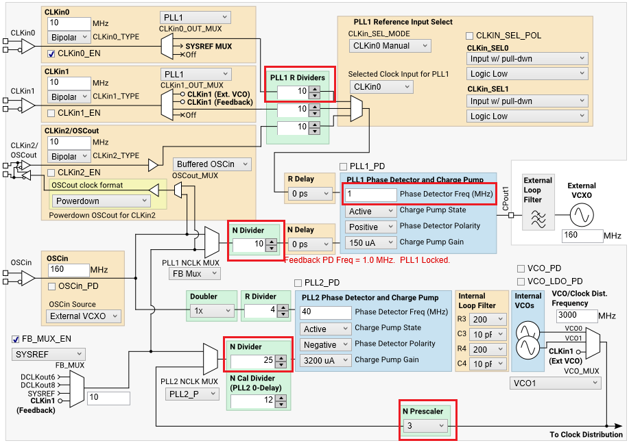
On our LMK04828 board, if in the dual loop mode, with below settings, PLL1 can be in lock consistently.


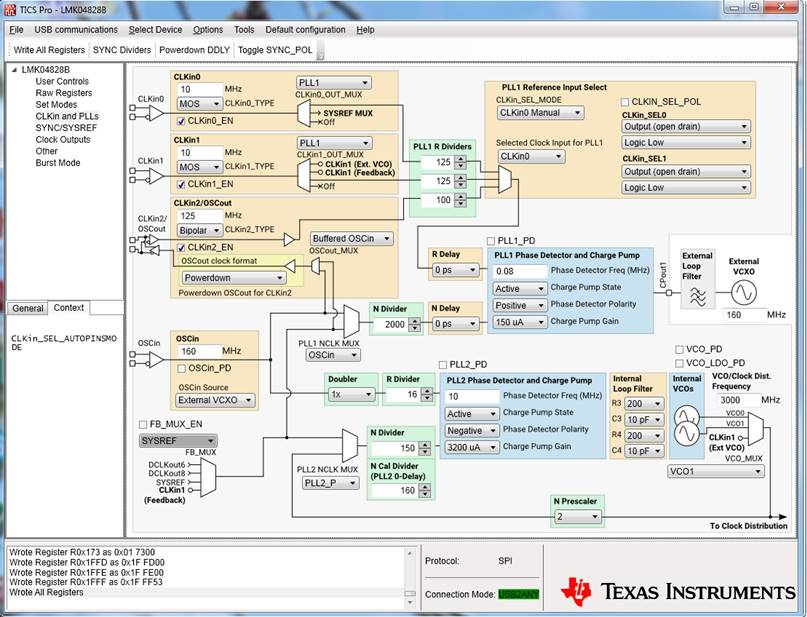
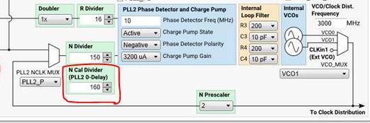
If on the Nested 0-Delay mode and kept the same PLL1 Fpd and charge pump setting, PLL1 can’t be in lock.

Until toggled the “PLL1_PD” or “PLL2_PD”, PLL1 can be in lock.   Actually toggling "FB_MUX_EN" also works.


Could you help to explain this issue? 


Thanks,

Jin

  • Hi Jin,

    In nested 0-delay mode, FB_MUX_EN needs to be enabled.

    Please see datasheet section 9.1.11, section 9.4.2 (Figure 19 and Table 7) for details.

    in TICS Pro, on the left column, you can select Set Modes and then click the Set Dual Loop 0-Delay Nested button to put TICS Pro in the nested mode. You will see the FB_MUX_EN will be enable automatically. 

  • Hi Noel,

    Maybe I didn't describe the issue clearly, I did have the "FB_MUX_EN" enabled in the nested 0-delay mode. And the nested 0-delay mode design worked fine at normal temperature.

    After the board heated up, the PLL1 couldn't be in lock after programmed with this nested 0-delay mode file.  

    While I deselected "FB_MUX_EN" then selected "FB_MUX_EN", the PLL1 was in lock.

    Actually, I tried with these actions also could make the PLL1 in lock:

    a. Select "PLL1_PD", then deselect "PLL1_PD"

    or

    b. Select "PLL2_PD", then deselect "PLL2_PD"

    Thanks,

    Jin

  • Hi Jin,

    I cannot explain why these actions can make it re-lock again.

    However, I do have some suggestion to your configuration, hopefully this change can fix your issue.

    Set PLL1 fpd to 1MHz; PLL2 fpd to 40MHz.

  • Hi Noel,

    Our design need to handle a variety of input/feedback frequencies and "Set PLL1 Fpd=1MHz" couldn't work.

    We need to understand why these actions is necessary to get in lock.

    Thanks,

    Jin  

  • Hi Jin,

    If PLL1 fpd cannot change, would you try using a higher charge pump current? 

    The input impedance of the Vtune pin of the VCXO is usually not very high, there is some leakage current when the charge pump is turned on. Increasing the fpd or charge pump current can relieve this problem. 

    I am not saying that the leakage is the root cause, I cannot explain the symptom that you have observed, I am proposing something that worth a try.

  • Hi Jin,

    PLL2 VCO need a successful calibration. But in 0-delay mode, the "N Cal Divider" has the wrong value 160, so the calibration can fail.

    Please modify it to 150.

    Programming register 0x168 starts a VCO calibration routine if PLL2_FCAL_DIS = 0.

    Hope this solve your problem.

    Regards,

    Shawn

  • Noel/Shawn, thanks for the suggestions!

    Noel,

    With Fpd=80KHz, I did try with increasing the CP current. Increasing CP current did shorten the lock time but not help the PLL1 lock issue. 

    Shawn,

    I corrected the "N Cal Divider" as you suggested but it didn't help to resolve the PLL1 lock issue.  

    Here attached the clock file I'm having issue on PLL1 lock.

    More detail about the PLL1 lock issue using the attached clock file if helps:

    1. After loaded the attached clock file, the LMK PLL1 can be in lock, if the board didn't heat up

    2. After loaded the attached clock file, the LMK PLL1 can not be in lock if the board already heated up

    3. The actions can make the PLL1 in lock:

    a. Switch the clock input for PLL1 from "CLKin1" to "CLKin0" , switch back the input of PLL1 to "CLKin1".  CLKin0 is not presented on board.

    or

    b. Select "PLL1_PD", then deselect "PLL1_PD"

    or

    c. Select "PLL2_PD", then deselect "PLL2_PD"

    or

    d. Deselect "FB_MUX_EN", then select "FB_MUX_EN"

    LMK04828B_B3000M_Nested_C0in10M_Cin10M_C2in125M_Fpd-80KHz.tcs

    Also could you provide the detail of how to calculate "N Cal Divider" on 0-delay mode?

    Thanks,

    Jin

  • Hi Jin,

    N Cal divider is dedicated for cascaded 0-delay mode, because calibration adopt different feedback clock path (from PLL2 VCO output) compared with final feedback path (from a final output clock with channel divider).

    For nested 0-delay mode, PLL2 VCO feedback path is fixed, so just copy N divider for N cal divider.

    For your case, when issue happened.

    1, Check PLL1 and PLL2 lock status.

    2, Check PLL1 holdover status (if PLL1 stay in holdover status, exit holdover time is hard to estimated because unknown frequency offset between reference frequency  and feedback frequency). This step is very important.

    Continue look into your configuration: It is in holdover_force.

    If holdover frequency is not critical, then disable HOLDOVER_EN. When lost reference, PLL2 will lock on VCXO free run frequency. It is easy for troubleshooting.

    If holdover function is needed, setting as below initial setting (still need optimize in a specialized case ).

    Attached tcs file for disable holdover.

    LMK04828B_B3000M_Nested_C0in10M_Cin10M_C2in125M_Fpd-80KHz-dis-Hold.tcs