This thread has been locked.
If you have a related question, please click the "Ask a related question" button in the top right corner. The newly created question will be automatically linked to this question.
Replies: 11
Views: 313
Part Number: LMK04208
Hi Team,
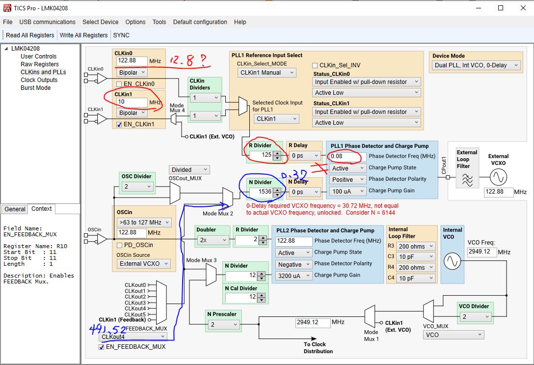
One of my customer is using LMK04208 for ZCU111 Xilinx RFSoC. The output Clock frequencies required is as below.
The inputs:
CLKIN0 -> 122.88 MHz
CLKIN1 -> terminated in connector
Customer requirement is: Feed 10MHz to CLKIN1. Do not use CLKIN0.
Customer have arrived on the values for the configuration they require. Can you please review/validate the attached configuration?
Regards, Shinu Mathew.
Configuration file attached.
PLL_Config.tcs
Thanks, Shinu Mathew.
In reply to Shinu.V.Mathew:
Hello Team,
Can you please help on this.
Can you please help on this request.
Regards, Shinu Mathew
The configuration has some problem for 0-delay feedback. Please clarify what's the synchronization requirement for 10 MHz input and other outputs.
Normally, we will adopt the lowest output frequency as the feedback clock, then other higher frequency clocks (= n * feedback clock, n is an integer) can be aligned on the same rising edges.
____________________________________________________________________________________
To design your own Clock Tree solution, visit WEBENCH Clock Architect !
More information Clock and Timing System products: http://www.ti.com/clock-and-timing/overview.html
In reply to Shawn Han:
Hi Shawn,
"Please clarify what's the synchronization requirement for 10 MHz input and other outputs”.
Not Sure what inputs you need for above point. Are you asking about the stratum level? Customer indeed want all the outputs to be synchronized to the inputs. Inputs are 12.8MHz and 10MHz. Output requirements are shared already.
Customer tried the attached configuration, 0-delay and dividers are fine.
However, they have trouble performing “switching between two clock inputs”.
When the other CLK (CLKIN0) is enabled, the PLL1 does not lock. PLL1 locks when only one of the clocks are enabled. Please note the R-divider is kept same for both inputs as recommended.
Please help to close this as early as possible.
Regards, Shinu.
1, Input the correct clocks for CLKin0 and CLKin1, find the Greatest Common Divisor (GCD) frequency for CLKin0 and CLKin1, which could be used for PLL1 phase detect frequency. Set CLKin Dividers and R divider for CLKin0 and CLKin1, if different CLKin Dividers can't get the same output frequency, then we need change R divider when switching to another CLKin.
2, Feedback clock: Select the lowest output frequency in all outputs need to be synchronized. Here 7.68 MHz may be your preferred.
3, Set N divider for PLL1 to achieve the same frequency as R divider path.
Thanks for the feedback.
Please find the attach file shared by customer can you please check and comment.
10M_CLKIN1_CLKIN0-DIS-NO-delay-Auto-CLKIN1-PLL1.tcs
10M_CLKIN1_CLKIN0-DIS-NO-delay-Auto-CLKIN1-PLL1.txt
3704.10M_CLKIN1_CLKIN0-DIS-NO-delay-Auto-CLKIN1-PLL1.tcs
4527.10M_CLKIN1_CLKIN0-DIS-NO-delay-Auto-CLKIN1-PLL1.txt
It can work, but why do not use CLKin0 or CLKin1 7.68 MHz as feedback clock ?
You suggested CLKIN0 or IN1 to br 7.68MHz? If yes, it is not possible. It has to be 12.8M (IN0) and 10M (IN1).
Or want CLKOUT0, CLKOUT1 as feedback clock?
Can you please clarify.