This thread has been locked.

If you have a related question, please click the "Ask a related question" button in the top right corner. The newly created question will be automatically linked to this question.

CDCE913: Register acces

Part Number: CDCE913

Hi,

I was trying to read registers from CDCE913 and values returned seemed wierd to me :

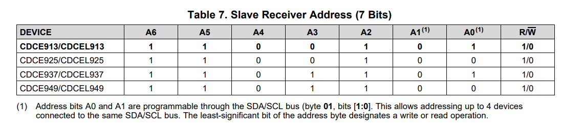
So I went on the forum and I vagly read the thread "CDCE913: I2C byte access to odd address" where I saw that register address where different than mines, like this :

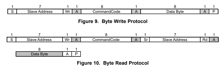
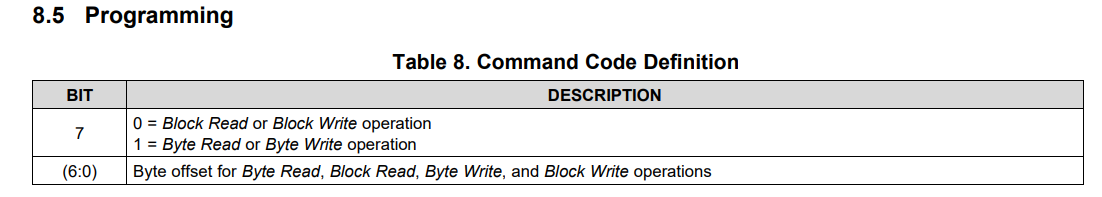
So I tried to add what seemed to be an offset of 0x80, and then I've got less wierd values :

Could you, please, tell me if the last values readed are the registers that I'm looking for ? (Generic Configuration Registers)

If so i'd like to change the slave address but I'd rather be sur it's the right register before writting anything

Regards,

Marine CHESSA

(P.S. : for now the device work porperly I just need to get the slave adress 0x65 free for an other device)

  • Pictures didn't follow, please find it in the file attachedCDCE913_valuesreadeddocx.docx

  • Hi Marine,

    I'm not sure if I understood your question correctly. But first, last two bits of I2C address are programmable: 

    Second, I2C read/write instructions are in the datasheet:

    For example, if you want to read back the value of register R5, you first write the device slave address, then a "0" for write, then write the address of R5 (0000 0101). Then repeated start sign, device slave address, a "1" for read, and the next byte you read back will be the register value.

    Regards,
    Hao

  • Hi Hao,

    I have a I2C bus, which is functionnal (I can read and write others devices on the bus)

    I'm also able to read CDCE913 registers.


    I know that I can change the slave address and that's what I'm aiming for.

    BUT when I read the register "0x01" the device answers "0x07"  ==> ok why not .... (by curiosity I also read others register as 0x02,0x03,...,0x06 answers were always "0x07" ==> wierd)

    As it was wierd I've search on the forum, and I saw that someone added some "offset" to registers adresses, instead of adressing "0x01" (=0b0000 00001) he was adressing "0x81" (=0b1000 0001).

    (https://e2e.ti.com/support/clock-and-timing/f/48/p/858572/3176365#3176365

    So I tried to use it to read my registers, I had the following answers

     read register 0x81 ==> 0x01

     read register 0x82 ==> 0xb4

     read register 0x83 ==> 0x01

     read register 0x84 ==> 0x02

     read register 0x85 ==> 0x50

     read register 0x86 ==> 0x0e

    Those answers seems more legit than "0x07"

    So my question is :
    When I send a "read" on the register address "0x81"  am I reading the "Generic Configuration Register 01h" ??
    Then can I write to this register with the confidence that it will do what I want ? And not affect the device fonction in an unwanted way ?

    Thank's by advance

    Marine

  • Hi Marine,

    Sorry for the late response. I believe that the "1" in bit 7 of 0b1000 0001 stands for read; and 0 is for write.

    To check if you wrote something correctly, you can choose a non-readonly register and see if you can read back what you write.

    Regards,
    Hao