This thread has been locked.

If you have a related question, please click the "Ask a related question" button in the top right corner. The newly created question will be automatically linked to this question.

LMK04828: rapid clock wander possibe between devices?

Part Number: LMK04828
Other Parts Discussed in Thread: TIDA-01021

Hello,

We're facing an issue trying to synchronize data converters on multiple boards.

We have several boards, each of them with two high-speed JESD-204B ADCs each. These boards have an LMK04828B as their clock generator/distributor for both ADCs. The ADC sampling clock is 2457,6 MHz, sent directly from the LMK04828B, output 10 for one ADC, output 12 for the other.

These LMK04828Bs on the ADC boards are configured in nested 0-delay mode. PLL1 has a Fpd of 1024 kHz and uses a Crystek CVHD-950 122,88 MHz VCXO. PLL2 has a Fpd of 122,88 MHz, with the reference coming directly from PLL1. The loop is internally closed from output 6, at 102,4 MHz, which is the lowest frequency for any output.

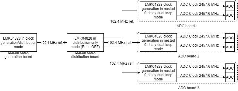
The PLL1 reference for these LMK04828Bs is external at 102,4 MHz and comes from a master clock distribution board, which also uses an LMK04828 in clock distribution mode (what comes from CLKIN1 goes to every DClk output, and whatever comes from CLKin0 is broadcast to the SDClk outputs.

The input from the master clock distribution board comes from the master clock generation board, which again uses an LMK04828B, which among other things generates the 102,4 MHz reference and SYSREF that goes to the clock distribution board and is distributed to every ADC clock.

Something like this:


The SYNC/SYSREF signal follows the same path. The master clock generation board self-synchronizes its outputs, then it broadcasts a SYNC pulse via the clock distribution board, causing the simultaneous alingment of all ADC board clock outputs, and then everything is reconfigured to switch to SYSREF functionality, and the JESD link goes up witth deterministic latency and our ADCs get time-synchronized and start sampling.

To test this, we insert a pulsed sinusoidal signal directly at the ADC inputs, coming from a signal generator using a splitter and relatively equal length cables. We trigger several thousands of simultaneous captures from all ADCs and analyze them. We see the pulsed signals and compare the skew between the instants when each captured pulse starts and ends. There, we see small invariant delays, which come from the length difference between the cables and such. This delay remains constant between captures with only residual variance. This system tolerates these skews and can compensate for them, so it's not an issue. As long as things remain deterministic and/or drift slowly enough, no problem.

However, we also check the phase relationship between the captured sines and there comes the issue. Between ADCs on the same ADC board, their phase shift between them within less than 0,1 degree peak to peak within captures and between captures, about 0,02 degrees RMS, with a noise-like shape. This is after removing the baseline phase shift (about 0,5º or so) likely caused by the signal splitter and the input balun of the ADC, and cable mismatch. On the other hand, between ADCs on different ADC boards we observe a rapid phase wander of +-3 degrees.

It is a phase wander, not a delay wander, as it remains constant with ADC input frequency, and it's not a drift, as it averages out to a baseline phase shift which remains constant between captures at the same input frequency. It bounces around aperiodically but not erratically, softly and gracefully dancing from -3 to 3º with respect to the baseline, with a maximum pseudo-oscillation frequency of about 200 Hz (we see mounds and valleys in the phase shift separated by a minimum of 5ms, with a soft, continous transition between them). Again, this phase wander is independent on the input ADC frequency. The higher the frequency the higher the baseline phase shift (linearly related, as there's a small delay) around where the phase dances about, but the wander awlays amounts to about 6de peak to peak independently of the frequency.

The ADCs are not TI parts but they use an architecture similar to some TI parts. The input, sampled at 2457,6 MHz at an intermediate frequency is downconverted to baseband with the ADC's internal downconverter, which employs an NCO clocked at the same ADC sampling clock. We  also have to syncrhonize the NCOs, but that seems to work well.

We've thought about what could be causing such a phase wander and we think it might be caused by clock wander between ADC sampling clocks at different ADC boards. We have checked the phase noise of the LMK04828's clock outputs and matches the expected profile and performance. We also measured the output clocks of two ADC boards simultaneously, but as our best scope currently on-hand only goes to 1 GHz, we had to measure a 245,76 MHz clock from each board, 10 times slower than the ADC sampling clock. After LMK04828 synchronization, they end up in phase with neglible delay between them, and there doesn't seem to be any appreciable wander between them. The scope tells us that if there's some wander (low freq. jitter), it's less than 15ps RMS between these divided clocks, but the scope isn't the best for this application and we can't get anything better in the current circumstances.

However, the true clock wander between LMK04828's in different ADC boards could be non-negligible. If the ADC didn't have an NCO that would create delay wander, but with the NCO in place it could also translate to phase wander. We're not seeing the delay wander as the sampled signal is decimated by a factor of 24, but things happening to the NCO which is clocked at the ADC sampling clock could be affecting.

We've seen several TI examples such as TIDA-01021 where you achieve very decent results with LMK04828's and even more PLL loops working together and with ADCs which also have an NCO, so we're not sure about what could be happening in our case. Do you have any clue about what might be happening?

Regards,

  • Hello David,

    First, apologies for the delay. Thanks for the very detailed post.

    To what is the PLL1 loop bandwidth set for the nested devices? You mentioned that the "pseudo-oscillation" is around 200Hz, which sounds like the order of magnitude I usually see for PLL1 loop bandwidth. PLL1 will track in-band wander, so if the loop bandwidth on PLL1 is set high enough I could see a noisy reference becoming an issue. If you aren't sure the exact loop bandwidth, we can simulate using PLLatinum Sim if we have the PLL1 charge pump gain and the loop filter parameters. You could also try reducing the charge pump gain to decrease the loop bandwidth, and see if the wander improves at all.

    Assuming the PLL1 loop bandwidth has something to do with it, this suggests that there might be some kind of spur at or below 200Hz being injected into the inputs of each card, potentially with a separate amplitude or with some kind of beat frequency between them. How have you configured the distribution mode device to provide a divide of 1? Are you using bypass mode on the output dividers, or are you using the divider with duty cycle correction?

    Another potentially quick test: if you change the distribution mode device to instead behave as a PLL2-only repeater (in cascaded zero-delay mode to preserve phase alignment), do things improve? I am wondering if there is some clock-to-clock skew that shows up in the 100MHz distribution mode case, which does not show up using a higher frequency VCO and dividing down; I place low likelihood on this possibility since I have tested the ~100MHz clock distribution mode case before and the sub-1kHz noise did not degrade in any way that would suggest the kind of phase wander you're seeing. But the test is pretty quick if you have easy access to the SPI bus.

    Speaking of the SPI bus, do you have any transactions on the bus connecting the LMK04828 while you're testing? If you do, is there a way to perform your test without the SPI transactions?

    What is the output format of the master clock distribution board (LVDS, LVPECL, etc)? Do you have a schematic of the output termination and the downstream nested device input termination? What mode is the input termination (Bipolar or MOS)? Theoretically, increasing the slew rate of the input to the nested devices would improve the close-in phase noise, and should improve any wander correlated with random noise. Maybe LMK04828 output format can be changed to increase LVPECL from 1.6V swing to 2V swing, or go from LVDS to HSDS, which would help test this theory.

    Another possibility is that there is power supply noise or ripple being injected into the PLL at or around the 200Hz point, which shows up as a spur. Likely candidates include mains supplies first through fourth harmonics, especially for off-line devices or power supplies. If power supply noise is the problem, switching to a different lower-noise supply or even a battery + LDO would likely show immediate improvements.

    I think that should be enough directions to get started for now. Let me know what you find out.

    Regards,

  • Hello Derek,

    Thanks for your answer, I forgot to update this post but about 1 hour after posting this it came to our mind that PLL1 could be a concern, and surely enough that was the root cause of the problem. We have already solved it, and I'm going to tell you how to get your opinion.

    Long story short, the first LMK04828 in the master clock generation board can take its reference either from a very high quality OCXO or from an external source which might be clean or not too much. In case of external reference, it goes through a special circuitery to convert whatever clock format you throw in to LVPECL with the sufficient slew rate without degrading the clock too much. The PFD of PLL1 for this one is 80 kHz and the loop bandwidth is set to 50 Hz. 

    The LMK04828s in the ADC boards were designed with a 20 Hz PLL1 filter, and that was causing the inter-board clock wander. Apparently it was too narrow and it didn't allow the ADC boards to track the close-in phase noise of the reference coming from the clock distribution board well enough. They were filtering the reference "too much" causing cummulative low frequency jitter effects between boards. In retrospective, we actually copy-pasted the design for this one from a different board and didn't think too much about it at the time, but it now seems like it was a poor choice.

    We tested and saw that doubling the bandwidth of the PLL1 loop filter for the ADC boards halved our wander issue. In the end, we set to a 900 Hz PLL1 loop filter (swapped components) and the issue is completely gone, now the ADCs within a board behave the same as ADCs between boards, staying within 0,02º RMS. We designed the filter for the highest CP current and with enough margin so that we can tweak the bandwith down if we want. We also upped the PFD from 1.024 MHz up to 34.3 MHz.

    This is sub-optimal, as the analysis shows that the LMK04828 in the ADC boards is actually not cleaning the jitter from the reference but actually worsening it a bit, but overall it's still good enough for the application. It seems like the noise profile of PLL1 was optimized for low bandwidth filters, so the PLL noise penalizes high bandwidth ones. We think that we'll use PLL2 only in the final product, as the reference coming from the master reference board is good enough and another LMK04828 can't clean if much further if at all.

    So, what are your thoughts about this? Does the solution we found make sense to you?

    EDIT: to clarify, this was all tested with the internal OCXO master reference, which is a 10 MHz 3ppb ultra low noise one with quite good phase noise specs. The external reference might be much worse, but at the same time much more stable. The VCXOs for PLL1 are CVHD-950's

  • Hi David,

    Okay, the loop bandwidth not tracking inter-board wander makes sense. I also think the solution you found makes sense for now, since essentially you are returning all sub-900Hz wander to in-band and tracking it out.

    At 900Hz loop bandwidth, the PLL1 noise is entirely dominated by 1/f noise. If your reference noise is worse than the PLL1 1/f noise, it isn't getting cleaned with 900Hz loop bandwidth anyway. And if it's better, then you don't need PLL1 in the first place, especially since your 102.4 MHz clock is already a relatively high-frequency integer divisor of your VCO frequency. I think in this case it makes sense to skip PLL1 entirely, and just run the ADC boards with PLL2-only zero delay instead. As an added benefit, you save some power and VCXO cost on the ADC boards.

    I wouldn't worry too much about the external reference source performance. Your circuit doing the EXTREF -> LVPECL conversion is already doing most of the work to clean up noise beyond 50Hz (assuming the VCO performance is good), and if the external reference has terrible close-in performance, I argue it isn't doing its job as an accurate external frequency reference. Even if the VCO performance on the EXTREF -> LVPECL isn't good, this is still a single point to implement possible improvements, vs. multiple devices across multiple ADC boards.

    Regards,

  • Hi Derek,

    That's exactly what we've seen doing the analysis, our solution works but close-in phase noise of our sampling clocks is now dominated by PLL1's noise. Fortunately, it's not a big deal for the application. It also tells us that we don't need the PLL1 at all, as any filter capable of minimally cleaning the reference would cause wander. As you said, most of the cleanup job is done by the master clock board, and cleanoup woudn't even be neccesary of we only used the internal OCXO reference.

    We were essentially swapping the natural low frequency wander of the reference clock for that of the VCXO of the first PLL of the ADC boards, which is uncorrelated among boards. We actually saw that with loop bandwidths above about 150 Hz the issue mostly disappeared, above that frequency the reference phase noise starts exiting the 1/f-ish zone and entering the plateau where the phase noise is much reduced, so not tracking it starts becoming less and less of an issue. 

    Thank you very much for your help and insights.

    Regards,

    David