This thread has been locked.

If you have a related question, please click the "Ask a related question" button in the top right corner. The newly created question will be automatically linked to this question.

LMK04821: convert SYSREF output to single-end to drive LMG1020

Part Number: LMK04821
Other Parts Discussed in Thread: LMG1020, LMK04832, LMK00804B, LMK00334

Hi team,

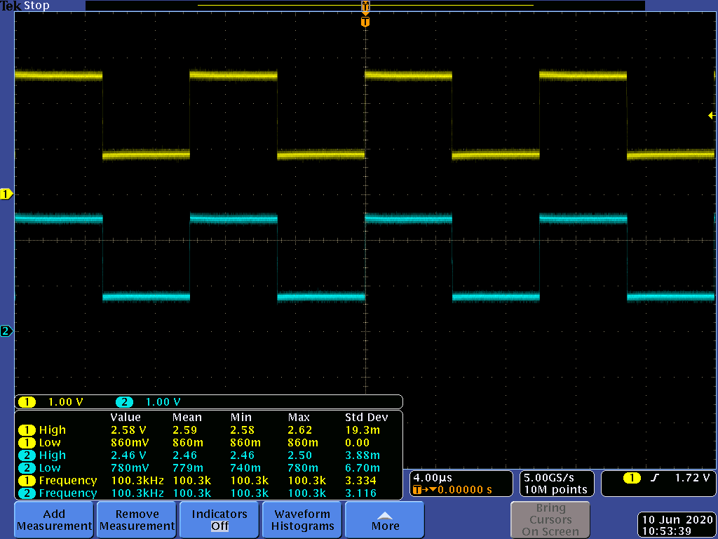
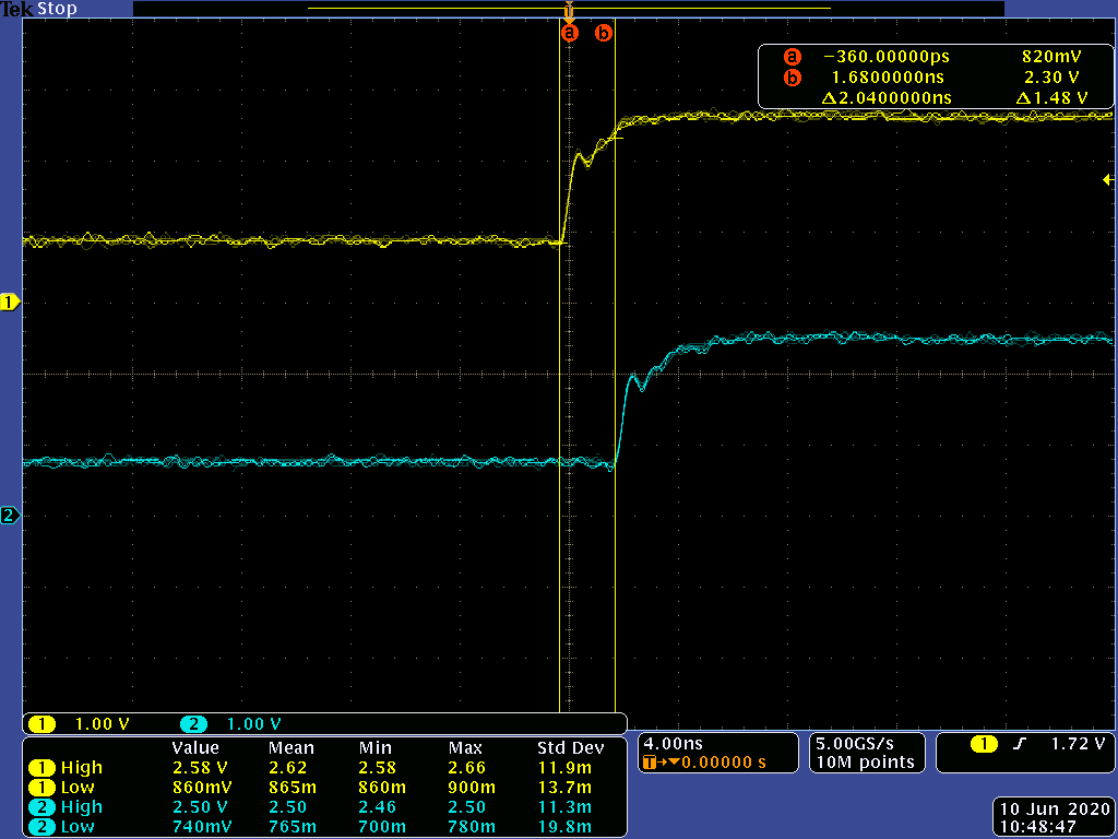
I'm trying to use LMK04821 SYSREF clock to generate a low jitter square wave to drive LMG1020. This is not a clock application, but a pattern generator. Below is output waveform of HSDS 8mA and DC coupling. The logic high/low voltage level is not sufficient to drive LMG1020, which I would like to make high voltage larger and low voltage smaller. Can I made it by resistance termination? I tried 3.5kohm termination with HSDS 8mA to get below result.  Or, do we have any level shift clock buffer that can convert the output to to single-end CMOS. The delay and additional jitter is the smaller the better.

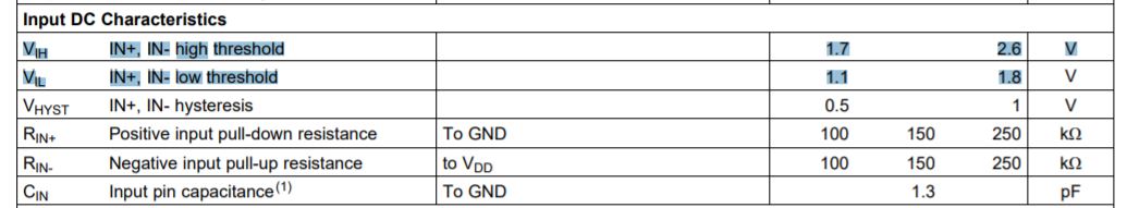
I attach the input thresholds for LMG1020 here. The accuracy of digital/analog delay of LMK04821 is much better than FPGA, so I'm trying to do this to drive LMG1020, replacing FPGA.

Thanks.

  • Hi Jerry,

    I recommend using the LMK04832 instead if possible. LMK04832 can also generate 100kHz SYSREF, and 9/14 outputs support single-ended or differential 3.3V CMOS.

    If LMK04832 isn't an option, you could instead drive LVPECL 1.6V AC-coupled into a balun, and bias the common-mode voltage of the balun to 2V. Depending on the balun impedance and turns ratio this could meet the required signal limit, as long as the balun frequency range permitted the target frequency and enough harmonics to make for sharp edges. Keep in mind that because the waveform is AC-coupled, the waveform would not be perfectly square, and the actual peak-to-peak voltage would be slightly more than 3.2V due to the AC-coupled wave overshoot and undershoot (example below, with assistance from Falstad circuit simulator - output waveform would be sqrt(2) * 1.6V by transformer turns ratio, but is actually just under 3.2V due to overshoot and undershoot).

    If only one output is needed from the LMK04821, you could also route the SYSREF output through the OSCout port using the feedback mux. LMK04821 OSCout supports single-ended CMOS.

    Regards,

  • Thank you, Derek.

    I see VCO0 of LMK04832 is 2500MHz and SYSREF divider is 8192 at max. I can only get a 300kHz SYSREF output. Instead, LMK04821 has a VCO divider. I attach the TICS Pro design for LMK04821 here.

    lmk04821-100kHz.tcs

    You could see the output from VCO divider is 500MHz, so that I can get an accurate 2ns phase delay between the two 100kHz CLKouts as below shows. This is what I mean to do. I'm not sure how much delay and jitter will be added by the balun, so I thought a high performance level shift clock buffer might help convert to CMOS voltage level without much additional delay and jitter.

    I see LMK04832 can straightly direct CLKin1 to SYSREF divider, bypassing PLLs and VCOs. This might be a solution for CMOS output. (*^_^*)

    Thanks. 

  • Hi Jerry,

    Generally I do not recommend trying to use two separate level shifter/CMOS buffers, since the part-to-part skew can vary considerably (usually several hundred picoseconds) compared to the channel-to-channel skew (tens of picoseconds). For LMG1020 where the exact pulse timing is very critical, part-to-part variation would probably be larger than acceptable. If you would still like to try the level shifter/CMOS buffer approach, the LMK00804B and the LMK00334 are both universal input, CMOS output devices.

    As you observed, the only way to get LMK04832 to 100kHz is by using the Fin port with a lower frequency than the integrated VCOs.

    Technically, LVPECL termination is 50Ω to 2V... With a clean and stable 3.3V supply, you could DC-terminate LMK04821 2V-LVPECL to the Thevenin equivalent of 2V 50Ω as below, which would just barely meet the VIH/VIL requirements:

    Regards,