A related question is a question created from another question. When the related question is created, it will be automatically linked to the original question.
If you have a related question, please click the "Ask a related question" button in the top right corner. The newly created question will be automatically linked to this question.
1. You are not getting the correct output because divide of one is an odd divide, and you must enable duty cycle correction for odd divides. Set DCLKout0_MUX, DCLKout2_MUX, and DCLKout10_MUX = 0x01 (Divider+DCC+HS).
2. How are you measuring the 100MHz output? Are you using a balun, or have you terminated the unused leg of the differential pair to 50Ω?
Can you tell me what synchronization procedure you are following? Note that section 9.3.3.1 of the datasheet explains the process of using the fixed digital delay to achieve a known phase offset between the outputs.
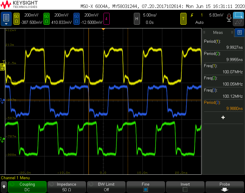
To confirm, you are referring to the distortion in this image:
Typically when I see this kind of distortion it has two common causes:
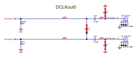
The other leg of the differential pair is unterminated. If output is LVDS for example, LVDS termination is 100Ω differential; both legs of the differential pair must see 50Ω to GND or 100Ω differential for proper termination.
The output is terminated improperly. The default termination for DCLKout0, for example, includes 240Ω to GND, which would disrupt standard LVDS behavior. LVDS termination is specified in datasheet section 10.4.2
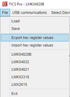
After confirming your desired settings in TICS Pro, you can use TICS Pro to export hex register values:
You can store the hex register programming in FPGA memory or read it in from some other external device. The register programming interface is a SPI bus which supports bidirectional read/write, see Figure 1 in the datasheet for the timing diagram.
For writing to the device, the SCK, CS*, and SDIO pins should be connected to FPGA SPI clock, chip select, and MOSI nets respectively. For reading from the device, you can either use a bidirectional transmitter on the MOSI net and switch to receive mode for SPI reads as the data bits are transmitted, or you can use 4-wire SPI mode by configuring one of the GPIO pins (PLL1_LD, PLL2_LD, CLKin_SEL0, CLKin_SEL1, or RESET pin) for SPI readback, and connecting the readback pin to the FPGA MISO line.
The LMK04828 I/O levels are 3.3V. While I don't have access to the schematics or EVM documentation (Xilinx requires login for this information), generally you have a few options for communicating with any FPGA:
Use a 3.3V I/O bank on the FPGA (Is I/O voltage control available on the bank or pins connected to the XADC pins?)
Use a 5V to 3.3V level shifter between the FPGA and the LMK04828
Use resistor dividers to reduce the 5V FPGA level to 3.3V, and use an open-drain transistor inverter to 5V + set LMK04828 readback GPIO output format to push-pull (inverted).
I got output clocks but those are not in SYNC and default it is taking as Divider value as 2(means External input clock is 100MHz then I'm getting output clock was 50MHz) but i want divider value should be 1(I/P clock 100MHz, O/P clock 100MHz).
How should i program DCLKout10_MUX = 0x01 (Divider+DCC+HS) and SYNC Divier - selection.
I you tell me register address and value, some solution for this dought.
The value of the DCLKout10_DIV (0x128[4:0]) should be set to 0x01 to ensure the divider value is 1. DCLKout10_MUX = 0x01 is correct for this mode.
You must follow the SYNC procedure outlined in the datasheet in order to align the outputs. Paraphrased, this looks like:
For each output you need to synchronize, set DCLKoutX_DDLY_CNTH and DCLKoutX_DDLY_CNTL. For example, if all output edges should be simultaneous, set DCLKoutX_DDLY_CNTH and DCLKoutX_DDLY_CNTL to the same values across all outputs. Also, ensure that DCLKoutX_DDLY_PD is cleared to 0 on all outputs you need to synchronize.
In the SYNC/SYSREF page, set the SYNC_MODE mux to pin mode (0x1), the SYSREF_MUX to normal SYNC (0x0), and the SYSREF_CLKin0_MUX to source from SYSREF_MUX (0x0).
Ensure SYNC_EN is set to 1.
For each output you need to synchronize, clear SYNC_DISx to 0.
Synchronize the dividers:
By pin: Apply an external signal HIGH to the SYNC pin, then LOW after at least seven CLKin1 clock cycles.
By software: Toggle the state of the SYNC_POL bit (0 -> 1 -> 0).
Set all SYNC_DISx bits to 1.
I have included a TICS Pro profile which accepts 100MHz on CLKin1 and should generate 100MHz on DCLKout0, SDCLKout1, DCLKout2, and DCLKout10.
I'm getting 40ps delay in between DCLKout0, DCLKout2, and DCLKout10. i Changed DCLKoutX_DDLY_CNTH and DCLKoutX_DDLY_CNTL register value also but there is no changes in that delay, what should i do?
can I do Same procedure for DAC038J84EVM? DAC Mode (LMFS=4211).
Each time you change the delay values (DCLKoutX_DDLY_CNTH/L), you must re-synchronize the LMK04828.
As far as I know, DAC38J84EVM is designed for use with the HSDC Pro software, which has its own configuration files included for LMK04828 based on DAC LMFS mode, and which uses the TSW14J56EVM to manage the synchronization procedure. That said, you could manually program the LMK04828, in which case the procedure described above would be applicable.
If you have further questions on DAC34J56EVM I recommend opening a separate E2E question specific to that EVM. The DAC team can offer more support for their EVM configurations and procedures.
Nice PPT I understood easily NO confusion after seeing PPT.
I'm getting 100MHz, 300MHz and 2400MHz when I used VCO0 that time it's not taking External Clock, it's taking on board clock, but i want to Generate with external 100MHz input clock not on board.
Take External Input Clock(100MHz) then Generate 100MHz and 2400MHz.
the Output of LMK should Depends on External Input (100MHz).
After getting output can you share me "CLKin and PLLs" Window and Remaning Windows Screenshot PPT.(same as previous format)
On the LMK04828, CLKin0/CLKin1/CLKin2 are connected as inputs only to PLL1. In order to get an external clock at 100MHz on CLKin1 to produce the desired signals, you will need to use PLL1 and drive a VCXO.
However, if your 100MHz signal is low-noise, you could instead directly drive the OSCin port. That way PLL1 is not required, and you do not need to use an external VCXO if you do not need one.
In the attached PPT below, I've included both options for your consideration. I did not go over the holdover page because it is not critical to operation, we can revisit the holdover page if it is needed. I also did not go over the "Other" page, because the I/O settings on this page are straightforward.
I've also attached the TICS Pro file I used to generate the configurations for PLL1+PLL2 option. The powerpoint explains how to modify the PLL1+PLL2 configuration to use PLL2 only.