This thread has been locked.

If you have a related question, please click the "Ask a related question" button in the top right corner. The newly created question will be automatically linked to this question.

CDCE6214-Q1: I2C Programming Issues

Part Number: CDCE6214-Q1
Other Parts Discussed in Thread: CDCE6214, CDCI6214,

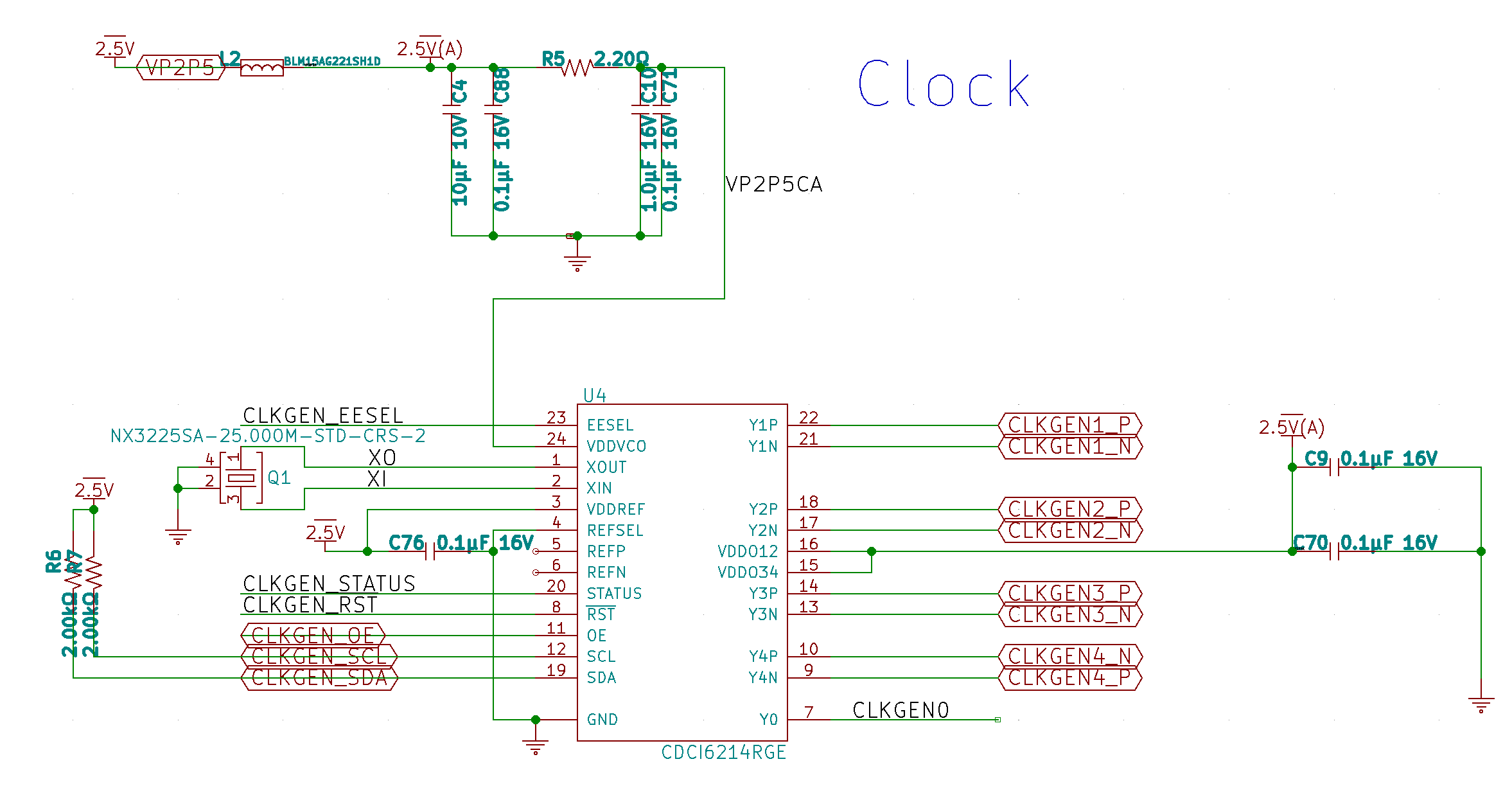
I am trying to use the CDCE6214 in I2C mode.

I have REFSEL tied directly to ground so it will power up in operational mode.  All the supplies are 2.5V.  I am looking for LVCMOS on output0 and LVDS on the other 4.  I have 3 prototypes of this system available, they all three behave the same.

PDN, SDA, SCL, HW_SW_CTRL, and GPIO4 are all driven from an FPGA.  GPIO1 is also connected to the FPGA, but right now the FPGA has that pin configured as an input.

If I set HW_SW_CTRL='1',  GPIO4(OE)='0', then change PDN from '1' to '0'.  I can communicate over I2C, I also see power supply current increase.

Here are the register values after PDN is cleared.

0x0053 (d83) = 0xFF00 
0x0052 (d82) = 0x05C0 
0x0051 (d81) = 0x0004 
0x0050 (d80) = 0x0008 
0x004F (d79) = 0x0008 
0x004E (d78) = 0x0000 
0x004D (d77) = 0x0002 
0x004C (d76) = 0x0188 
0x004B (d75) = 0x8248 
0x004A (d74) = 0xA241 
0x0049 (d73) = 0x0000 
0x0048 (d72) = 0x0006 
0x0047 (d71) = 0x0406 
0x0046 (d70) = 0x0898 
0x0045 (d69) = 0xA241 
0x0044 (d68) = 0x0000 
0x0043 (d67) = 0x0006 
0x0042 (d66) = 0x0006 
0x0041 (d65) = 0x4AD8 
0x0040 (d64) = 0xA241 
0x003F (d63) = 0x0000 
0x003E (d62) = 0x0006 
0x003D (d61) = 0x0000 
0x003C (d60) = 0x6028 
0x003B (d59) = 0x8248 
0x003A (d58) = 0x5032 
0x0039 (d57) = 0x0000 
0x0038 (d56) = 0x0006 
0x0037 (d55) = 0x001E 
0x0036 (d54) = 0x3400 
0x0035 (d53) = 0x0069 
0x0034 (d52) = 0x5000 
0x0033 (d51) = 0x40C0 
0x0032 (d50) = 0x01C0 
0x0031 (d49) = 0x0013 
0x0030 (d48) = 0x1A05 
0x002F (d47) = 0x0280 
0x002E (d46) = 0x0000 
0x002D (d45) = 0x4F80 
0x002C (d44) = 0x0318 
0x002B (d43) = 0x0051 
0x002A (d42) = 0x0002 
0x0029 (d41) = 0x0000 
0x0028 (d40) = 0x0000 
0x0027 (d39) = 0x0000 
0x0026 (d38) = 0x0000 
0x0025 (d37) = 0x0000 
0x0024 (d36) = 0x0000 
0x0023 (d35) = 0x0028 
0x0022 (d34) = 0x0000 
0x0021 (d33) = 0x0000 
0x0020 (d32) = 0x0000 
0x001F (d31) = 0x0000 
0x001E (d30) = 0x0030 
0x001D (d29) = 0x0000 
0x001C (d28) = 0x0000 
0x001B (d27) = 0x0004 
0x001A (d26) = 0x0000 
0x0019 (d25) = 0x0400 
0x0018 (d24) = 0x091C 
0x0017 (d23) = 0x2406 
0x0016 (d22) = 0x00A2 
0x0015 (d21) = 0x0503 
0x0014 (d20) = 0x0000 
0x0013 (d19) = 0x0000 
0x0012 (d18) = 0x0000 
0x0011 (d17) = 0x26C4 
0x0010 (d16) = 0x921F 
0x000F (d15) = 0xA037 
0x000E (d14) = 0x0000 
0x000D (d13) = 0x0000 
0x000C (d12) = 0x0000 
0x000B (d11) = 0x0000 
0x000A (d10) = 0x0000 
0x0009 (d09) = 0x274C 
0x0008 (d08) = 0x0001 
0x0007 (d07) = 0x0C2D 
0x0006 (d06) = 0x0DEC 
0x0005 (d05) = 0x0008 
0x0004 (d04) = 0x0000 
0x0003 (d03) = 0x0200 
0x0002 (d02) = 0x0000 
0x0001 (d01) = 0x7652 
0x0000 (d00) = 0x2000

Two things I notice.  Register 0 is 0x2000.  Pretty sure it should be 0x1000.  Register 3 indicates a CRC fault.  Not sure this is normal.

I have a configuration I developed in TICS Pro.  I export the register settings and try to write them to the CDCE6214.  The third column is the read back value after writing the value from the second column to the address in the first column.

0x0053 = 0xFD00 0xFF00 
0x0052 = 0x01C0 0x05C0 
0x0051 = 0x0004 0x0004 
0x0050 = 0x0000 0x0000 
0x004F = 0x0000 0x0000 
0x004E = 0x1000 0x1000 
0x004D = 0x0000 0x0000 
0x004C = 0x0188 0x0188 
0x004B = 0x8008 0x8008 
0x004A = 0xA181 0xA181 
0x0049 = 0x0000 0x0000 
0x0048 = 0x0006 0x0006 
0x0047 = 0x0006 0x0006 
0x0046 = 0x0008 0x0008 
0x0045 = 0xA181 0xA181 
0x0044 = 0x0000 0x0000 
0x0043 = 0x0006 0x0006 
0x0042 = 0x0006 0x0006 
0x0041 = 0x0808 0x0808 
0x0040 = 0xA181 0xA181 
0x003F = 0x0000 0x0000 
0x003E = 0x0006 0x0006 
0x003D = 0x0000 0x0000 
0x003C = 0x6008 0x6008 
0x003B = 0x8008 0x8008 
0x003A = 0x502C 0x502C 
0x0039 = 0x0002 0x0002 
0x0038 = 0x0006 0x0006 
0x0037 = 0x001E 0x001E 
0x0036 = 0x3400 0x3400 
0x0035 = 0x0069 0x0069 
0x0034 = 0x5000 0x5000 
0x0033 = 0x40C0 0x40C0 
0x0032 = 0x01C0 0x01C0 
0x0031 = 0x0013 0x0013 
0x0030 = 0x1A14 0x1A14 
0x002F = 0x0A00 0x0A00 
0x002E = 0x0000 0x0000 
0x002D = 0x4F80 0x4F80 
0x002C = 0x0318 0x0318 
0x002B = 0x0051 0x0051 
0x002A = 0x0002 0x0002 
0x0029 = 0x0000 0x0000 
0x0028 = 0x0000 0x0000 
0x0027 = 0x0000 0x0000 
0x0026 = 0x0000 0x0000 
0x0025 = 0x0000 0x0000 
0x0024 = 0x0000 0x0000 
0x0023 = 0x0028 0x0028 
0x0022 = 0x0000 0x0000 
0x0021 = 0x0000 0x0000 
0x0020 = 0x0000 0x0000 
0x001F = 0x0000 0x0000 
0x001E = 0x0030 0x0030 
0x001D = 0x0000 0x0000 
0x001C = 0x0000 0x0000 
0x001B = 0x0004 0x0004 
0x001A = 0x0000 0x0000 
0x0019 = 0x0400 0x0400 
0x0018 = 0x0718 0x0718 
0x0017 = 0x0406 0x2406 
0x0016 = 0x00A2 0x00A2 
0x0015 = 0x0503 0x0503 
0x0014 = 0x0000 0x0000 
0x0013 = 0x0000 0x0000 
0x0012 = 0x0000 0x0000 
0x0011 = 0x26C4 0x26C4 
0x0010 = 0x921F 0x921F 
0x000F = 0xA037 0xA037 
0x000E = 0x0000 0x0000 
0x000D = 0x0000 0x0000 
0x000C = 0x0000 0x0000 
0x000B = 0x0000 0x0000 
0x000A = 0x0000 0x0000 
0x0009 = 0x0000 0x274C 
0x0008 = 0x0001 0x0001 
0x0007 = 0x0C0D 0x0C2D 
0x0006 = 0x0E2C 0x0DEC 
0x0005 = 0x0008 0x0008 
0x0004 = 0x0040 0x0040 
0x0003 = 0x0000 0x0000 
0x0002 = 0x0000 0x0000 
0x0001 = 0x2660 0x2660 
0x0000 = 0x100C 0x2000

You can see here address 0 did not change.  I know the reset bit should clear itself, but the GPIO directions still seem incorrect.

I can also read the EEPROM.  Here are those results if it helps.

EE Addr 0x0000 (00) = 0x7002 
EE Addr 0x0001 (01) = 0x487F 
EE Addr 0x0002 (02) = 0x1B12 
EE Addr 0x0003 (03) = 0x0000 
EE Addr 0x0004 (04) = 0x28A0 
EE Addr 0x0005 (05) = 0x4CD0 
EE Addr 0x0006 (06) = 0x0700 
EE Addr 0x0007 (07) = 0x6680 
EE Addr 0x0008 (08) = 0x8320 
EE Addr 0x0009 (09) = 0x5A24 
EE Addr 0x000A (10) = 0x6C24 
EE Addr 0x000B (11) = 0x122D 
EE Addr 0x000C (12) = 0x1626 
EE Addr 0x000D (13) = 0x4909 
EE Addr 0x000E (14) = 0x0434 
EE Addr 0x000F (15) = 0x0102 
EE Addr 0x0010 (16) = 0xA801 
EE Addr 0x0011 (17) = 0x00EC 
EE Addr 0x0012 (18) = 0x4000 
EE Addr 0x0013 (19) = 0x2470 
EE Addr 0x0014 (20) = 0x0200 
EE Addr 0x0015 (21) = 0x0060 
EE Addr 0x0016 (22) = 0x0000 
EE Addr 0x0017 (23) = 0x0000 
EE Addr 0x0018 (24) = 0x0000 
EE Addr 0x0019 (25) = 0x0A22 
EE Addr 0x001A (26) = 0x1800 
EE Addr 0x001B (27) = 0x00D8 
EE Addr 0x001C (28) = 0x8000 
EE Addr 0x001D (29) = 0x0C40 
EE Addr 0x001E (30) = 0x0000 
EE Addr 0x001F (31) = 0x0C48 
EE Addr 0x0020 (32) = 0x0000 
EE Addr 0x0021 (33) = 0x0D08 
EE Addr 0x0022 (34) = 0x0000 
EE Addr 0x0023 (35) = 0x1008 
EE Addr 0x0024 (36) = 0x0000 
EE Addr 0x0025 (37) = 0x0000 
EE Addr 0x0026 (38) = 0x0000 
EE Addr 0x0027 (39) = 0x1000 
EE Addr 0x0028 (40) = 0xA440 
EE Addr 0x0029 (41) = 0x00EC 
EE Addr 0x002A (42) = 0x4000 
EE Addr 0x002B (43) = 0x2470 
EE Addr 0x002C (44) = 0x0200 
EE Addr 0x002D (45) = 0x0060 
EE Addr 0x002E (46) = 0x0000 
EE Addr 0x002F (47) = 0x0000 
EE Addr 0x0030 (48) = 0x0000 
EE Addr 0x0031 (49) = 0x0A22 
EE Addr 0x0032 (50) = 0x1800 
EE Addr 0x0033 (51) = 0x00D8 
EE Addr 0x0034 (52) = 0x0000 
EE Addr 0x0035 (53) = 0x0C50 
EE Addr 0x0036 (54) = 0x0000 
EE Addr 0x0037 (55) = 0x0C50 
EE Addr 0x0038 (56) = 0x0000 
EE Addr 0x0039 (57) = 0x0D10 
EE Addr 0x003A (58) = 0x0000 
EE Addr 0x003B (59) = 0x1100 
EE Addr 0x003C (60) = 0x0000 
EE Addr 0x003D (61) = 0x0000 
EE Addr 0x003E (62) = 0x0000 
EE Addr 0x003F (63) = 0x0000

I notice the CRC register is all 0's so it is probably no wonder the CRC compare is failing.

I am stuck.  I have tried several things but I can't get it to generate the required outputs.  It seems like a programming problem.  Have you seen anything like this?

  • A few more notes:

    The input is a 25MHz 8pF 100Ω crystal on SECREF with no additional series resistance or loading caps.

    PRIREF is unconnected.

    Power supplies are all 2.5V, but they do use recommended filtering between them.

    We used a very similar circuit on a previous design with the CDCI6214 and were able to program it without issue.  The only major difference beside the part number was REFSEL was pulled low with a 10kΩ to ground.  On the new design REFSEL is wired directly to ground.

  • Now I see that if I write register 0 to 0x1000 or 0x1008 (without the reset) it works and I read back 0x1000 or 0x1008.

    Next if I write 0 to 0x1004 with the reset bit, it returns 0x2000 on the next read.  

    I looks like something is going wrong in the reset process and reconfiguring registers.

  •  Not much here, but you are welcome to evaluate.  All the labeled connections are routed to an FPGA.

    Also, my register file from TICS Pro.

    SimlaClockRegisterValues.txt
    R85	0x00550000
    R84	0x00540000
    R83	0x0053FD00
    R82	0x005201C0
    R81	0x00510004
    R80	0x00500000
    R79	0x004F0000
    R78	0x004E1000
    R77	0x004D0000
    R76	0x004C0188
    R75	0x004B8008
    R74	0x004AA181
    R73	0x00490000
    R72	0x00480006
    R71	0x00470006
    R70	0x00460008
    R69	0x0045A181
    R68	0x00440000
    R67	0x00430006
    R66	0x00420006
    R65	0x00410808
    R64	0x0040A181
    R63	0x003F0000
    R62	0x003E0006
    R61	0x003D0000
    R60	0x003C6008
    R59	0x003B8008
    R58	0x003A502C
    R57	0x00390002
    R56	0x00380006
    R55	0x0037001E
    R54	0x00363400
    R53	0x00350069
    R52	0x00345000
    R51	0x003340C0
    R50	0x003201C0
    R49	0x00310013
    R48	0x00301A14
    R47	0x002F0A00
    R46	0x002E0000
    R45	0x002D4F80
    R44	0x002C0318
    R43	0x002B0051
    R42	0x002A0002
    R41	0x00290000
    R40	0x00280000
    R39	0x00270000
    R38	0x00260000
    R37	0x00250000
    R36	0x00240000
    R35	0x00230028
    R34	0x00220000
    R33	0x00210000
    R32	0x00200000
    R31	0x001F0000
    R30	0x001E0030
    R29	0x001D0000
    R28	0x001C0000
    R27	0x001B0004
    R26	0x001A0000
    R25	0x00190400
    R24	0x00180718
    R23	0x00170406
    R22	0x001600A2
    R21	0x00150503
    R20	0x00140000
    R19	0x00130000
    R18	0x00120000
    R17	0x001126C4
    R16	0x0010921F
    R15	0x000FA037
    R14	0x000E0000
    R13	0x000D0000
    R12	0x000C0000
    R11	0x000B0000
    R10	0x000A0000
    R9	0x00090000
    R8	0x00080001
    R7	0x00070C0D
    R6	0x00060E2C
    R5	0x00050008
    R4	0x00040040
    R3	0x00030000
    R2	0x00020000
    R1	0x00012660
    R0	0x0000100C
    

  • Possibly I found it.

    In an act of desperation I cut the ground trace to REFSEL.  

    I can now program the part and see the clocks running as I expect.

    Can you confirm that connecting REFSEL directly to ground would cause problems?

    It seems to be even worse on the CDCI6214.  We tried that part with this circuit and it shorted SDA to ground permanently and drew ~100mA @ 2.5V.

    Apparently REFSEL is doing more on these parts than the data sheet describes.

    Also, with REFSEL floating can I configure the EEPROM so it powers up operational, or am I now stuck re-programming after every power cycle?

  • Hi Barry,

    First of all, one quick question: does everything work well when you use Ticpsro?

    Second, I was about to suggest starting from fallback mode, where both REFSEL and EEPROMSEL are floating.

    REFSEL doesn't have to be floating. Try register REFSEL_SW. 

    Even if REFSEL is floating, the EEPROM can still be programmed and used. Pin EEPROMSEL selects EEPROM pages (0 or 1).

    Regards,
    Hao

  • We do not have the hardware required to connect directly to TICS Pro.  If the TICS Pro hardware pulls REFSEL or floats REFSEL, then it would mask this issue.

    We built 4 prototypes of this circuit initially with the CDCI6214.  They all failed horribly.  SDA was always grounded after applying power and current consumption was very high.  An earlier board with REFSEL pulled low, worked fine with the CDCI6214.

    We replaced all 4 parts with CDCE6214-Q1 devices.  One board was lost to rework issues.  The I2C interface now worked on all 3 remaining boards, but a soft reset would fail and reset register 0 to 0x2000 on all 3 boards.  I have not found any documentation on this failure mode.

    I cut the trace to REFSEL and the CDCE6214-Q1 operates as expected.

    I suggest you tie REFSEL to ground with very low resistance and test this case.  I am confident it is an issue with the part with a simple workaround.

  • Is there any way to exit fall-back mode without cycling power?

    I think I remember why we tied REFSEL low to avoid fall-back mode.   It seems you have to write all the registers to make the part functional from fall-back mode.

    Now that I cut the REFSEL to GND trace I always power up in fall-back and the EEPROM seems useless.

    I thought cycling the PDN pin would resample EEPROMSEL and I could exit fall-back, but it looks like a real power down is required.  Correct?

  • Toggling the PDN pin will have the same effect as a power cycle. Also, you can still use EEPROM when REFSEL is low. Both REFSEL and EEPROMSEL must be floating in order to enter fallback mode.

    Regards,
    Hao

  • This is how I am testing PDN operation. (updated with actual polarities)

    I power the board with REFSEL and EEPROMSEL floating and enter fall-back mode as expected with PDN=1.

    In fall-back mode I can write the registers and transfer them to EEPROM.  So far so good.

    Now I set PDN='0' and EEPROMSEL='1'.  The device enters reset and I cannot read I2C registers.  This is expected.

    I set PDN='1' while holding EEPROMSEL='1' hoping it will enter Serial Interface Mode.  I can now read the I2C registers, but using the fall-back I2C slave address which indicates the device is still in fall-back mode.  It will not answer to the serial mode address, and the registers were not refreshed from the EEPROM.

    I get the same results from two different devices.

    I think PDN rising does not re-evaluate REFSEL or EEPROMSEL.  

    Should I be doing it differently?

  • Hi Barry,

    I'm pretty sure that toggling PDN reloads the EEPROM content to registers or has the device re-enter fallback. But maybe you're right that the EEPROMSEL and REFSEL levels are not re-sampled.

    There are two things:

    1. You don't have to write EEPROM in fallback mode. You can do that in EEPROM page 1 (see table 20 of datasheet), because by default EEPROM page 0 is configured as pin mode, where I2C is disabled.

    2. You don't have to float REFSEL pin. I don't know why floating this pin made things work, but normally you shouldn't have to do so. The reference selection can be controlled by either pin or register. The register control has higher priority. See table 1 of datasheet for details.

    Regards,
    Hao

  • Hao,

    Thank you for considering my questions and responding.

    1. I understand you do not have to program the EEPROM.  I wanted to use EEPROM if possible rather than reprogram after every power cycle.  With REFSEL and EEPROMSEL floating at power up, you can never apply the EEPROM contents to the registers.  The data sheet never mentions if cycling PDN resamples REFSEL and EEPROMSEL, my testing shows it does not.

    2. I understand REFSEL can be pulled low (or high).  My discovery is that you cannot tie REFSEL directly to ground.  The CDCx6214 are not functional with REFSEL tied directly to ground.  I recommend you tie it to ground with 0Ω to test this yourself, or at least simulate it.

    Thanks,

  • Hi Barry,

    Understood. Thanks for the comments. Let me know if there're other questions.

    Regards,
    Hao