This thread has been locked.

If you have a related question, please click the "Ask a related question" button in the top right corner. The newly created question will be automatically linked to this question.

CDCI6214: REFSEL setting for EEPROM access

Expert 3795 points
Part Number: CDCI6214

Dear e2e Support,

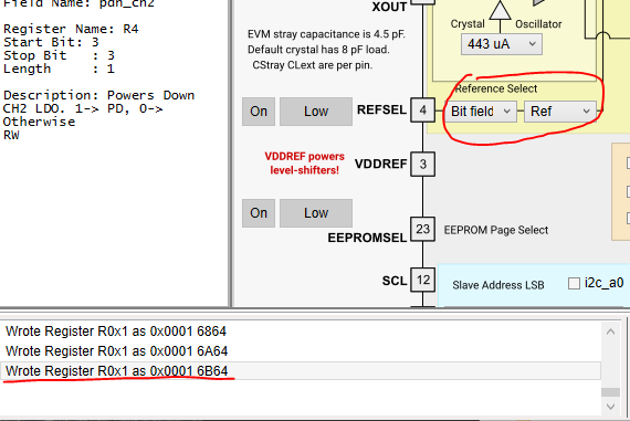
For a hardware reason on his PCB, my customer has fixed the REFSEL pin to '1'.

Considering this pin state, could you tell us if it's still possible to get access to the EEPROM?

It's said p.28 of our datasheet that we are supposed to be in high impedance, but I've seen on the forum that the high state could work.

Regards,

  • Hi there,

    Yes you can still access EEPROM. Just need to make sure that EEPROMSEL = high otherwise you won't be able to access I2C by default.

    Regards,
    Hao

  • Hi,

    I am the customer in question. Thank you for your reply!

    So if I understand well, if I want to access to the EEPROM I just need to follow the procedure described page 28 & 29 with REFSEL = 1 and EEPROMSEL = 1 instead of using the mid-level? In this case, which slave address do I have to use? The datasheet specifies 0x74 but it corresponds to the case where EEPROMSEL = MID, so I guess the slave address should rather be 0x77 in my case, isn't it?

    To be honest I will not use the EEPROM in the first place, I will start by simply configure the circuit using the I2C interface at each power up. I wanted to know wether this functionality would be available for the future.

    In short, I have to set EEPROMSEL to 1 after a reset and make sure to use the correct slave address (0x77). Then I configure each register according to my application and I stop there without any interaction with the EEPROM. Could you confirm that?

    Again, thank you for the support.

    Maxime

  • Hello Maxime,

    Yes. When you set EEPROMSEL = HIGH, you will need to adjust your slave address accordingly as per Table 12 on page 27 of the datasheet.

    You will need to change the slave address to either 0x76 or 0x77 based on the I2C_A0 (Configuration Bit in EEPROM Page 1, default value of 1).

    Thanks,

    Vibhu

  • Hi,

    Thank your for the explanation! 

    I have other questions about the configuration.

    To help me find the correct settings I installed TICS Pro software. Thanks to the user controls and the block diagram panels, the circuit is configured according to my hardware constraints and my needs. Most registers are OK but some of them are "reserved" registers and the default settings are not always the same as in the datasheet.

    For example, CH1_CTRL4 register as the default value 0679h and I want to set ch1_glitchless_en bit high. This means that 067Ah is the new value. Yet in the raw register panel of the sotfware, the value for this register with my setup is 0851h. 

    Should I write this value in the register?

    Or should I write the default value with the modification (0679h + 0001h)?

    Or should I first read the register and only change the value of the last bit?

    This is not the first reserved register I see with a different value that the default one. Is this normal?

    Thank you, best regards

  • Hi Maxime,

    The best of way of doing it is to read back the register values from default EEPROM page 1, then change the fields as needed.

    Regards,
    Hao

  • Hello,

    Ok thank you.

    I am currently trying to do this but I encountered some issues. When I write the slave address 0x77 (EEPROMSEL = 1) the CDCI6214 doest not acknoledge back (checked on the oscilloscope and by my acknoledgment error program).

    There is a power-up procedure in the datasheet for EEPROM access. But I don't want to access to the EEPROM. Should I also use this procedure to write directely into the registers using I2C? 

    Or could I just power-up the device without doing a reset and configure it using I2C?

    Thank you. 

  • Hi,

    That is a typo in the datasheet. The I2C address should be 0x76 for both EEPROM pages. It is better to start with EEPROM because there're hidden registers that you wouldn't want to change. You can just power up from EEPROM page 1 and write I2C without reset or anything.

    Regards,
    Hao

  • Ah! 

    Ok, thank you for the tip. The communication works well using 0x76 slave address (EEPROMSEL=1), I can read the acknoledgments.

    But I am still facing serious initialization problems. First I tried to write only a few registers to configure CH0 as an active output and shut down CH1-CH4. The aim was to verify the circuit and the communication work well. At the end of the I2C transactions, OE (GPIO4) pin is set to 1. I didn't work.

    So I did what you suggested to me before: I read all the registers, then I modified only the fields needed to power-up CH0 (and setup GPIO directions) in order not to interfer with reserved bits and it didn't work neither. Note that I used the block diagram on TICS Pro to enable CH0 and see what registers needed to be modified (minimalizing the risk of error).

    Joined to this message is an Excel sheet with the register values at different states of the process (firt column are the register values after a power-up on EEPROM page 1, second column are the registers I wrote, and third column are the read values of all registers).

    Hardware setup: input clock on REF pins is 10 MHz LVDS with 900 mV amplitude (measured). All the power supplies are 2.5V, EEPROMSEL=1, REFSEL=1 (tied to VDD). 

    I tried on two different boards and the results are the same.

    Did I missed something?

    Thank you 

    debug_cdci6214.xlsx

  • Hi,

    The Y0 configuration looks correct to me. The only thing that I'm not sure I understand is 0x0001 6824. Can you try the following (to use PRIREF by register setting):

    Which corresponds to 6B64.

    Regards,
    Hao

  • Hi,

    0x0001 6824 is used to select the REF clock using the dedicated pin and to set up GPIO4 as OE pin. GPIO1 is defined here as OE1 input but it dosn't matter as I defined this GPIO as output in the following register. 

    I tried last week to set ref_mux_src to 1 and ref_mux to 1 with 0x0001 6B24 and as far as I can remember I didn't work either. So I did it again this afternoon and it still doesn't work.

    Maybe a stupid question but, does the input clock need to be running before setting the registers?

    Another question, did you have any feedback about REFSEL pin hardware setup? On my design, it is directly tied to VDD (2.5V). Is there any problem with this?

    I really don't know what to do now. I will carried on others tests tomorrow... 

    Thank you for your help

  • Hi,

    I did new tests this morning, without success.

    This time I tried to modify 4 registers from the default EEPROM page 1 configuration to define REF input as AC-differential instead of LVCMOS and CH1 as an LVDS output instead of HCSL. Here are the values of the registers:

    0x001A 8A1C

    0x0026 0405

    0x003A 0000

    0x003B 1061

    At the end of I2C transaction (read all the registers to check if write sequence worked), GPIO1 (pin 20) is set to 1 because it has the OE1 function. 

    I investigated all the signals with an oscilloscope and there is a strange behaviour on the input stage of REF clock. The differential voltage accoss the 100 ohm resistor (before the two AC-coupling 100 nF capacitors) is 900 mV, which is fine. But after the two capacitors, the two signals are zero-centered which is curious. There should be an input voltage bias, isn't it? It is as if the input stage was not powered. 

    All the VDD pins (VDDREF, VDDVCO, VDDO12, VDDO34) are connected to 2.5 V in my design.

    I hope to find the solution as soon as possible... :( 

    Regards

  • I don't see any problem tying the REFSEL pin to VDD (through >1kOhm current limiting resistor). In fact, when R1 is set that way, PRIREF is selected by the register bit so the REFSEL pin level doesn't matter. 

    No you don't need a reference clock to program the chip. There's internal state machine clock for that purpose. 

    Can you try this:

    1. Power up the chip from REFSEL = floating and EEPROMSEL = floating (fallback mode). That way the chip boots up from a known state (silicon default)

    2. Then dump the registers exported from Ticspro (you can do File -> export hex registers).

    Regards,
    Hao

  • Hi,

    REFSEL is connected to VDD without current limiting resistor. But yes I can bypass this function using the ref_mux bit-field configuration.

    Unfortunately I can't try the sequence you are proposing me because I have no control over the REFSEL pin since it is hardware connected to VDD without resistor. Even with EPPROMSEL = Z, REFSEL state will follow VDD voltage during the power-up, so I don't know the device will be able to enter in fallback mode. Anyway, I can try.

    I found something during a few experimentation. It seems that I'm having timing issues after the power-up sequence of the board. There is a 20 ms timer between the enable of the 2.5V LDO and the rise of RESETN. The 2.5V voltage rise in 14.5 ms, so there is a 5.5 ms margin before RESETN goes to 1 (in the datasheet the initialization time after POR is given at 5 ms). But as soon as RESETN = 1, the state machine goes directly into I2C writing and that is too quick. I added a intermediate VIO to manually control the timing between RESETN = 1 and the start of I2C transactions and that is better. Now I can measure the biais voltage on the REF input. 

    I modified a few registers to

    - power down CH3 (0x0004 00FD)

    - set the REF input as AC-differential (0x001A 8A1C)

    - change CH1 output into LVDS (0x0026 0405)

    - specify VDD voltage to 2.5V for LVDS (0x0028 0000)

    I got a signal on the output but it is very low amplitude (35-40 mV differential voltage and 1.35 V common-mode voltage) and the frequency is around 95 MHz. It is obviously not what I should have. 

    The default setup on EEPROM page 1 is 100 MHz output from a 25 MHz crystal clock (x4), so I should get a 40 MHz signal since my input clock is 10 MHz.

    That's a little step forward!

  • Hi,

    The frequency cannot scale like that because with 40MHz input, the VCO frequency will be out of range. As far as I remember, the default VCO frequency is 2.4GHz (or maybe 2.5GHz), which is 100x the XTAL frequency. Now 100 * 10MHz = 1GHz which is way out of VCO range so it won't work.

    Regards,
    Hao

  • Hi,

    Oh, what a rookie mistake... I was focused on other settings and I completely forgot to set up the PLL correctly. 

    I have adjusted pll_ndiv, pll_psfb, pll_psa and ch1_iod_div to get a 80 MHz output frequency from the 10 MHz input clock.

    I have also added large timers between all power-up steps to make sure there are not timing issues. Now everything is working fine, it only needs optimization. 

    Thanks for the support.

    I hope this topic will help other users in the future.