This thread has been locked.

If you have a related question, please click the "Ask a related question" button in the top right corner. The newly created question will be automatically linked to this question.

LMK05028: LMK05028 Application Issue when Spur Comes with REF Input

Part Number: LMK05028
Other Parts Discussed in Thread: LMK04821

Hi Team,

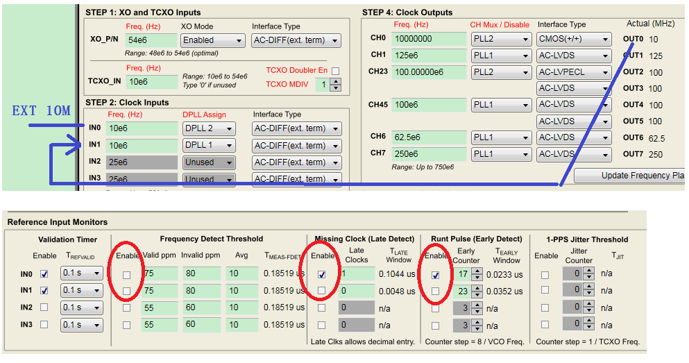
My customer is using LMK05028. We found one unlock issue. The REF input is 10M. And when there is a spur locate at 30.72M and the power is ~-40dBm, the LMK05028 is unlock. When remove the spur, it locked again. We suspect that the device's rejection of the spur is not strong enough. Need to check with you, if there is a way to increase the rejection of the spur's influence at LMK05028 side. Thanks!

  • Hello, 

    How is the spur "removed"? This implies we know what is the source of the spur, so I need to know what it was to introduce it. 

    Secondly, when mentioning unlock, we need to clearly what was unlocked. I assume this is only looked at witch the output connected to an equipment, so when unlock implies the device is no longer outputting. This would mean APLL has gone out of lock after locking, which doesn't make any sense. 

    I'm emphasizing this because DPLL can also go unlock, for example when the reference is removed, and the output should maintain because APLL is locked. 

    So please provide what is the source of the spur and how were you able to remove it. Secondly, what specifically is going "unlock". 

    Thanks and regards,

    Amin 

  • Hi Amin,

    Sorry for the misunderstanding. This spur is from another clock device coupling by space. And removed by switching off the clock device. By saying "unlock", I mean that the DPLL2 is unlocked. We also set the 0xBB to be 0xd, but it seems that it didn't work, the DPLL2 is still unlock when spur comes.

    We want to know if there is a config that can avoid the unlock when spur comes.Thanks.

  • Hi, 

    So the spur observed at an output from the DPLL2/APLL2 loop, causes DPLL2 to be unlocked? This spur is from another device that's on the board. Is this device close to the reference input? 

    To understand what's causing the DPLL2 to unlock, we need to know a few things, is the reference DPLL2 trying to lock to, valid? Does DPLL2 select that reference? Here's the GUI image where this data can be found, if you hover over it it will also tell you register numbers and bits that correspond to this info: 

    If the reference is invalid - we'd need to understand what part of the validation checks is causing to become invalid when the spur is there. 

    If it is valid, the DPLL should be locked unless it's a bad configuration. Which shouldn't be the case since you mentioned if there's no spur the DPLL is locked. 

    Thanks and regards,

    Amin 

  • Hi Amin,

    30.72M comes to the device by the REFIN0 and you can find the tcs files as attached.

    When there is no spur and input 10M 0dBm reference into REFIN0, the register status is as below:

    0x2E6 -- 0x30 

    0x2FF-- 0x02

    0x303--0x01

    DPLL2 loss of lock: 0  DPLL2 lock

    DPLL2  REF0 selected 1 selected 

    When there is 30.72M spur and input 10M 0dBm reference into REFIN0, the register status is as below:

    0x2E6 -- 0x20

    0x2FF-- 0x02

    0x303--0x00

    DPLL2 loss of lock: 1  DPLL2 unlock

    DPLL2  REF0 selected

    After removing the 30.72 spur, the register status change to the status in the 1st step(no spur status).

  • lmk05028 BTS 10Hz 1013.tcs

    LMK05028 BTS 10Hz 1013 .txt
    R0	0x000010
    R1	0x00010B
    R2	0x000235
    R3	0x000301
    R4	0x0004FF
    R5	0x0005FF
    R6	0x0006DF
    R7	0x0007BF
    R8	0x000802
    R9	0x000900
    R10	0x000AC0
    R11	0x000B00
    R12	0x000C3B
    R13	0x000D22
    R14	0x000ED0
    R15	0x000F00
    R16	0x001000
    R17	0x001100
    R18	0x001200
    R19	0x001300
    R20	0x001400
    R21	0x001500
    R22	0x001600
    R23	0x001700
    R24	0x001800
    R25	0x001900
    R26	0x001A0F
    R27	0x001B55
    R28	0x001C55
    R29	0x001D00
    R30	0x001E00
    R31	0x001F00
    R32	0x002000
    R33	0x002105
    R34	0x002205
    R35	0x002334
    R36	0x002403
    R37	0x002500
    R38	0x002611
    R39	0x002702
    R40	0x0028CE
    R41	0x002900
    R42	0x002ABF
    R43	0x002B00
    R44	0x002C11
    R45	0x002D11
    R46	0x002E06
    R47	0x002F4E
    R48	0x003066
    R49	0x003170
    R50	0x003203
    R51	0x003300
    R52	0x00343F
    R53	0x003502
    R54	0x003600
    R55	0x003700
    R56	0x003800
    R57	0x00396E
    R58	0x003A10
    R59	0x003B00
    R60	0x003C00
    R61	0x003D08
    R62	0x003E18
    R63	0x003F10
    R64	0x004020
    R65	0x004100
    R66	0x00420B
    R67	0x004310
    R68	0x004410
    R69	0x004500
    R70	0x004600
    R71	0x00470A
    R72	0x004810
    R73	0x004900
    R74	0x004A00
    R75	0x004B0F
    R76	0x004C10
    R77	0x004D00
    R78	0x004E00
    R79	0x004F00
    R80	0x005000
    R81	0x005104
    R82	0x005200
    R83	0x005300
    R84	0x005401
    R85	0x005512
    R86	0x005612
    R87	0x005712
    R88	0x00583F
    R89	0x005903
    R90	0x005A02
    R91	0x005B03
    R92	0x005C44
    R93	0x005D0F
    R94	0x005E17
    R95	0x005F05
    R96	0x006002
    R97	0x006103
    R98	0x006244
    R99	0x00630F
    R100	0x006417
    R101	0x006505
    R102	0x006600
    R103	0x00672E
    R104	0x00684B
    R105	0x0069DA
    R106	0x006A12
    R107	0x006BF6
    R108	0x006C85
    R109	0x006D03
    R110	0x006E00
    R111	0x006F01
    R112	0x007000
    R113	0x007100
    R114	0x007200
    R115	0x007300
    R116	0x007400
    R117	0x007500
    R118	0x007600
    R119	0x007700
    R120	0x007800
    R121	0x007900
    R122	0x007A00
    R123	0x007B00
    R124	0x007C02
    R125	0x007D00
    R126	0x007E01
    R127	0x007F01
    R128	0x008077
    R129	0x008100
    R130	0x008232
    R131	0x0083ED
    R132	0x008409
    R133	0x00857B
    R134	0x008642
    R135	0x00875F
    R136	0x008803
    R137	0x008900
    R138	0x008A01
    R139	0x008B00
    R140	0x008C00
    R141	0x008D00
    R142	0x008E00
    R143	0x008F00
    R144	0x009000
    R145	0x009100
    R146	0x009200
    R147	0x009300
    R148	0x009400
    R149	0x009500
    R150	0x009600
    R151	0x009702
    R152	0x009800
    R153	0x009901
    R154	0x009A01
    R155	0x009B77
    R156	0x009C00
    R157	0x009D00
    R158	0x009E03
    R159	0x009F0D
    R160	0x00A029
    R161	0x00A100
    R162	0x00A20D
    R163	0x00A329
    R164	0x00A424
    R165	0x00A5BB
    R166	0x00A6FF
    R167	0x00A700
    R168	0x00A800
    R169	0x00A900
    R170	0x00AA00
    R171	0x00AB00
    R172	0x00AC00
    R173	0x00AD00
    R174	0x00AE00
    R175	0x00AF00
    R176	0x00B009
    R177	0x00B1A3
    R178	0x00B292
    R179	0x00B3DB
    R180	0x00B4EA
    R181	0x00B529
    R182	0x00B633
    R183	0x00B755
    R184	0x00B8F4
    R185	0x00B900
    R186	0x00BA10
    R187	0x00BB95
    R188	0x00BC15
    R189	0x00BD0D
    R190	0x00BE09
    R191	0x00BF01
    R192	0x00C001
    R193	0x00C100
    R194	0x00C200
    R195	0x00C342
    R196	0x00C400
    R197	0x00C500
    R198	0x00C642
    R199	0x00C700
    R200	0x00C800
    R201	0x00C91B
    R202	0x00CA00
    R203	0x00CB00
    R204	0x00CC1B
    R205	0x00CD10
    R206	0x00CE00
    R207	0x00CF00
    R208	0x00D02C
    R209	0x00D100
    R210	0x00D200
    R211	0x00D326
    R212	0x00D400
    R213	0x00D500
    R214	0x00D615
    R215	0x00D700
    R216	0x00D800
    R217	0x00D915
    R218	0x00DA01
    R219	0x00DB02
    R220	0x00DCEE
    R221	0x00DD03
    R222	0x00DE20
    R223	0x00DF02
    R224	0x00E0EE
    R225	0x00E103
    R226	0x00E220
    R227	0x00E302
    R228	0x00E426
    R229	0x00E502
    R230	0x00E658
    R231	0x00E702
    R232	0x00E826
    R233	0x00E902
    R234	0x00EA58
    R235	0x00EB00
    R236	0x00EC00
    R237	0x00ED1C
    R238	0x00EE41
    R239	0x00EFCC
    R240	0x00F000
    R241	0x00F198
    R242	0x00F296
    R243	0x00F381
    R244	0x00F400
    R245	0x00F51C
    R246	0x00F641
    R247	0x00F7CC
    R248	0x00F800
    R249	0x00F998
    R250	0x00FA96
    R251	0x00FB81
    R252	0x00FC00
    R253	0x00FD46
    R254	0x00FEA4
    R255	0x00FF7E
    R256	0x010000
    R257	0x010198
    R258	0x010296
    R259	0x010381
    R260	0x010400
    R261	0x010546
    R262	0x0106A4
    R263	0x01077E
    R264	0x010800
    R265	0x010998
    R266	0x010A96
    R267	0x010B81
    R268	0x010C0A
    R269	0x010D0A
    R270	0x010E0A
    R271	0x010F0A
    R272	0x011000
    R273	0x011100
    R274	0x011200
    R275	0x011300
    R276	0x011400
    R277	0x011500
    R278	0x011600
    R279	0x011700
    R280	0x011800
    R281	0x011900
    R282	0x011A00
    R283	0x011B00
    R284	0x011C00
    R285	0x011D00
    R286	0x011E00
    R287	0x011F00
    R288	0x012000
    R289	0x012100
    R290	0x012200
    R291	0x012300
    R292	0x012410
    R293	0x012580
    R294	0x012600
    R295	0x012700
    R296	0x012805
    R297	0x012901
    R298	0x012A80
    R299	0x012B00
    R300	0x012C00
    R301	0x012D01
    R302	0x012E3D
    R303	0x012F0A
    R304	0x013000
    R305	0x013100
    R306	0x013200
    R307	0x013301
    R308	0x013400
    R309	0x013501
    R310	0x013600
    R311	0x013700
    R312	0x013800
    R313	0x013900
    R314	0x013A00
    R315	0x013B00
    R316	0x013C00
    R317	0x013D00
    R318	0x013E06
    R319	0x013F8B
    R320	0x014000
    R321	0x014100
    R322	0x014200
    R323	0x014303
    R324	0x0144E8
    R325	0x0145A0
    R326	0x01460C
    R327	0x014702
    R328	0x014802
    R329	0x01490F
    R330	0x014A00
    R331	0x014B00
    R332	0x014C00
    R333	0x014D0A
    R334	0x014E0E
    R335	0x014F0A
    R336	0x01500F
    R337	0x015108
    R338	0x01520F
    R339	0x01530D
    R340	0x01540B
    R341	0x01550D
    R342	0x015600
    R343	0x015700
    R344	0x015800
    R345	0x0159B0
    R346	0x015A01
    R347	0x015BB1
    R348	0x015C02
    R349	0x015D8E
    R350	0x015E09
    R351	0x015F01
    R352	0x016000
    R353	0x01612C
    R354	0x016217
    R355	0x01630F
    R356	0x016417
    R357	0x016501
    R358	0x016600
    R359	0x016720
    R360	0x016827
    R361	0x016902
    R362	0x016A01
    R363	0x016B00
    R364	0x016C00
    R365	0x016D00
    R366	0x016E21
    R367	0x016F55
    R368	0x017055
    R369	0x017155
    R370	0x017255
    R371	0x017355
    R372	0x0174FF
    R373	0x0175FF
    R374	0x0176FF
    R375	0x0177FF
    R376	0x0178FF
    R377	0x017924
    R378	0x017A00
    R379	0x017B0A
    R380	0x017C00
    R381	0x017D0E
    R382	0x017EA6
    R383	0x017F00
    R384	0x018000
    R385	0x018198
    R386	0x018296
    R387	0x018380
    R388	0x018400
    R389	0x018514
    R390	0x018600
    R391	0x018702
    R392	0x0188EE
    R393	0x018900
    R394	0x018A00
    R395	0x018B1E
    R396	0x018C84
    R397	0x018D80
    R398	0x018E00
    R399	0x018F00
    R400	0x019000
    R401	0x019100
    R402	0x019200
    R403	0x019300
    R404	0x019402
    R405	0x019500
    R406	0x019603
    R407	0x0197E8
    R408	0x01988C
    R409	0x019900
    R410	0x019A00
    R411	0x019B00
    R412	0x019C00
    R413	0x019D00
    R414	0x019E00
    R415	0x019F00
    R416	0x01A000
    R417	0x01A100
    R418	0x01A200
    R419	0x01A300
    R420	0x01A400
    R421	0x01A500
    R422	0x01A600
    R423	0x01A700
    R424	0x01A800
    R425	0x01A900
    R426	0x01AA00
    R427	0x01AB00
    R428	0x01AC00
    R429	0x01AD00
    R430	0x01AE00
    R431	0x01AF00
    R432	0x01B000
    R433	0x01B100
    R434	0x01B200
    R435	0x01B300
    R436	0x01B400
    R437	0x01B500
    R438	0x01B600
    R439	0x01B700
    R440	0x01B800
    R441	0x01B93D
    R442	0x01BA0A
    R443	0x01BB00
    R444	0x01BC00
    R445	0x01BD00
    R446	0x01BE01
    R447	0x01BF00
    R448	0x01C000
    R449	0x01C100
    R450	0x01C200
    R451	0x01C300
    R452	0x01C400
    R453	0x01C500
    R454	0x01C600
    R455	0x01C700
    R456	0x01C800
    R457	0x01C906
    R458	0x01CA8B
    R459	0x01CB00
    R460	0x01CC00
    R461	0x01CD00
    R462	0x01CE04
    R463	0x01CF4C
    R464	0x01D0B0
    R465	0x01D10F
    R466	0x01D202
    R467	0x01D302
    R468	0x01D40F
    R469	0x01D500
    R470	0x01D600
    R471	0x01D700
    R472	0x01D80A
    R473	0x01D90E
    R474	0x01DA0A
    R475	0x01DB0F
    R476	0x01DC08
    R477	0x01DD0F
    R478	0x01DE0D
    R479	0x01DF0B
    R480	0x01E00D
    R481	0x01E100
    R482	0x01E200
    R483	0x01E300
    R484	0x01E4B0
    R485	0x01E501
    R486	0x01E6B1
    R487	0x01E702
    R488	0x01E88E
    R489	0x01E909
    R490	0x01EA01
    R491	0x01EB00
    R492	0x01EC2C
    R493	0x01ED17
    R494	0x01EE0F
    R495	0x01EF17
    R496	0x01F001
    R497	0x01F100
    R498	0x01F220
    R499	0x01F327
    R500	0x01F402
    R501	0x01F501
    R502	0x01F600
    R503	0x01F700
    R504	0x01F800
    R505	0x01F924
    R506	0x01FAAA
    R507	0x01FBAA
    R508	0x01FCAA
    R509	0x01FDAA
    R510	0x01FEAA
    R511	0x01FFFF
    R512	0x0200FF
    R513	0x0201FF
    R514	0x0202FF
    R515	0x0203FF
    R516	0x020424
    R517	0x020500
    R518	0x02060A
    R519	0x020700
    R520	0x02080D
    R521	0x020951
    R522	0x020A18
    R523	0x020B00
    R524	0x020C98
    R525	0x020D96
    R526	0x020E88
    R527	0x020F00
    R528	0x021014
    R529	0x021100
    R530	0x021202
    R531	0x0213A9
    R532	0x0214D2
    R533	0x021500
    R534	0x02161E
    R535	0x021784
    R536	0x021886
    R537	0x021900
    R538	0x021A00
    R539	0x021B00
    R540	0x021C00
    R541	0x021D00
    R542	0x021E00
    R543	0x021F02
    R544	0x022000
    R545	0x022104
    R546	0x02224C
    R547	0x02238F
    R548	0x022400
    R549	0x022500
    R550	0x022600
    R551	0x022700
    R552	0x022800
    R553	0x022900
    R554	0x022A00
    R555	0x022B00
    R556	0x022C00
    R557	0x022D00
    R558	0x022E00
    R559	0x022F00
    R560	0x023000
    R561	0x023100
    R562	0x023200
    R563	0x023300
    R564	0x023400
    R565	0x023500
    R566	0x023600
    R567	0x023700
    R568	0x023800
    R569	0x023900
    R570	0x023A00
    R571	0x023B00
    R572	0x023C00
    R573	0x023D00
    R574	0x023E00
    R575	0x023F00
    R576	0x024000
    R577	0x024100
    R578	0x024200
    R579	0x024300
    R580	0x024404
    R581	0x024504
    R582	0x024600
    R583	0x024700
    R584	0x024800
    R585	0x024900
    R586	0x024A00
    R587	0x024B00
    R588	0x024C00
    R589	0x024D00
    R590	0x024E00
    R591	0x024F00
    R592	0x025000
    R593	0x025100
    R594	0x025200
    R595	0x025300
    R596	0x025400
    R597	0x025500
    R598	0x025600
    R599	0x025700
    R600	0x025800
    R601	0x025900
    R602	0x025A2C
    R603	0x025BC4
    R604	0x025C55
    R605	0x025D4C
    R606	0x025E49
    R607	0x025F49
    R608	0x026082
    R609	0x02612D
    R610	0x026245
    R611	0x026345
    R612	0x026440
    R613	0x026500
    R614	0x026600
    R615	0x026700
    R616	0x02686E
    R617	0x026900
    R618	0x026AC0
    R619	0x026B44
    R620	0x026C16
    R621	0x026D0E
    R622	0x026E83
    R623	0x026F10
    R624	0x02700C
    R625	0x027109
    R626	0x027200
    R627	0x027300
    R628	0x027400
    R629	0x027500
    R630	0x027600
    R631	0x027705
    R632	0x027801
    R633	0x027900
    R634	0x027A00
    R635	0x027B00
    R636	0x027C01
    R637	0x027D00
    R638	0x027E00
    R639	0x027F00
    R640	0x028000
    R641	0x028100
    R642	0x028205
    R643	0x028301
    R644	0x028400
    R645	0x028500
    R646	0x028600
    R647	0x028701
    R676	0x02A400
    R677	0x02A500
    R678	0x02A640
    R681	0x02A944
    R682	0x02AA44
    R683	0x02AB44
    R684	0x02AC44
    R685	0x02AD44
    R686	0x02AE44
    R687	0x02AF04
    R688	0x02B044
    R691	0x02B300
    R715	0x02CB00
    R716	0x02CC04
    R717	0x02CD04
    R718	0x02CE04
    R719	0x02CF04
    R736	0x02E000
    R741	0x02E500
    R742	0x02E610
    R764	0x02FC00
    R766	0x02FE00
    R767	0x02FF00
    R770	0x030200
    R771	0x030301
    R775	0x030700
    R776	0x030800
    R784	0x031000
    R785	0x031100
    
    PFA the tcs config

  • Hello, 

    Thank you for the information and sharing the .tcs file. So when the spur is there, it's IN0 is no longer valid. 

    I noticed in your .tcs file that IN0 can support either DPLL1 or DPLL2 based off of inputs however for DPLL reference selection only IN0 has a priority. If this is changed, the DPLL2 can lock to IN1 as well. How to update the priority selection in the GUI with image at the bottom of the email. 

    The question of why IN0 becomes invalid and IN1 remains valid is understood now as well. IN0 has PPM detector enabled. Not sure what the requirements for the system are... but you can disable IN0 PPM detector or at least increase the invalid threshold. The spur is causing enough noise where this is becoming invalid. 

    On a similar note, I would advise that missing clock is enabled - there's no harm in this and it would allow DPLL to realize a loss of reference much faster and enter holdover before corruption or large frequency error can occur. 

    Thanks and regards,

    Amin 

    DPLL2 Auto Priority change: 

    PPM detect and missing (late/early) clock detect 

  • Hi Amin,

    1. LMK05028 IN0 from EXT 10MHz input,lmk05028 IN1 from lmk05028 out0 10MHz 1/2  Vpp, so we can just check DPLL2 IN0.

    2. You can find the tcs file as attached (lmk05028 BTS 10Hz fae 1016)

    disable Valid IN0,

    Enable  missing clock (when late clocks =0, input check is valid, so set it to 1 )

    Enable  runt pulse 

    3. When there is no spur and input 10M 0dBm reference into REFIN0, the register status is as below:

    0x2E6 -- 0x30 

    0x2FF-- 0x02

    0x303--0x01

    DPLL2 loss of lock: 0  DPLL2 lock

    DPLL2  REF0 selected : 1 selected 

    4. When there is 30.72M spur, reg is as below(no change of the reg,DPLL2 unlock):

    0x2E6 --0x30

    0x2FF-- 0x02

    0x303--0x01

    DPLL2 loss of lock: 1  DPLL2 unlock

    DPLL2  REF0 selected : 1 selected 

    When switch off the spur, the reg recover to the status when there is no spur

    5. When enable missing clock late clocks=0, and 10M 0dBm ref input to refin0 and no spur:

    0x2E6 -- 0x20 

    0x2FF-- 0x02

    0x303--0x00

    DPLL2 loss of lock: 0  DPLL2 lock

    DPLL2  REF0 selected : 0

    lmk05028 BTS 10Hz ae 1016.tcs

  • Hello, 

    Thanks for the details. I would just like to confirm I understand correctly: 

    1. No spur - DPLL1 selects REF1 and DPLL2 selects REF0 - both locked 
    2. Spur added - DPLL1 selects REF1 and locked - DPLL2 has REF0 as valid and selected, but DPLL2 is not locked
      1. This is with no input validation enabled basically, correct? Since next step is saying Late and Early enabled.. I'm assuming this is with no PPM detector and no missing clock, so really input may be valid but in actuality we're not running it through any validation
    3. Final case: Enabling missing/early - only REF1 is considered valid (REF0 isn't valid) - DPLL1 selects REF1 and is locked - DPLL2 is showing locked yet the reference selection is "holdover" 
      1. Loss of lock is only tied to frequency lock and therefore will no get flagged if device was previously locked 

    One more thing I've noticed, why is the output type CMOS (+/+) yet input is AC-DIFF(ext. Term). CMOS (+/+) would provide outputs with both n and p in phase.

    • If using singled ended input, you can change the selection to LVCMOS and the change the channel output to CMOS (+/Hi-Z) or vice versa since only 1 channel would be needed. 
    • If using differential, then output type should be changed to a differential type (LVDS, CML, LVPECL) 

    Thanks and regards,

    Amin 

  • Hi, 

    One more thing that's confusing, the picture is contradicting what I've took to understand. OUT0 is feeding IN1 which is going to DPLL1 - so OUT0 cannot impact DPLL2 in any way. In the picture you have DPLL2 is just using IN0 which is an external reference. 

    The output type update still applies though - OUT0 CMOS (+/+) will be worse in terms of both performance and spur as well. So perhaps that change can fix the system. 

    Thanks and regards,

    Amin 

  • Hi Amin,

    Please see the response as below:

    Thanks for the details. I would just like to confirm I understand correctly: 

    1.    No spur - DPLL1 selects REF1 and DPLL2 selects REF0 - both locked   

    —— yes

    2.    Spur added - DPLL1 selects REF1 and locked - 

    ——  Spur added - DPLL1: lock; DPLL1 ref1 selected :lock (when frequency detect threshold disable,if  enable is unlock)

         DPLL2 has REF0 as valid and selected, but DPLL2 is not locked

    ——Spur added - DPLL2: unlock; DPLL2 ref0 selected :lock (when frequency detect threshold disable,if  enable is unlock)

    1.    This is with no input validation enabled basically, correct?

    ——  yes

     Since next step is saying Late and Early enabled.. I'm assuming this is with no PPM detector and no missing clock, so really input may be valid but in actuality we're not running it through any validation

    —— frequency detect threshold disable, Late and Early enabled :  the result  same ;Spur added and frequency detect threshold enable,the DPLL2 REF0 selected  :invalid

    3.    Final case: Enabling missing/early - only REF1 is considered valid (REF0 isn't valid) -DPLL1 selects REF1 and is locked -

                ——   yes

       DPLL2 is showing locked yet the reference selection is "holdover" 

       ——   Spur added,DPLL2 showing  unlock,APLL2 is lock ; DPLL2 reference selection  "holdover" 

    1.    Loss of lock is only tied to frequency lock and therefore will no get flagged if device was previously locked 

    —— yes

    One more thing I've noticed, why is the output type CMOS (+/+) yet input is AC-DIFF(ext. Term). CMOS (+/+) would provide outputs with both n and p in phase.

    ——one CMOS+ to lmk05028 IN1, other cmos+ to lmk04821 refin0

    o  If using singled ended input, you can change the selection to LVCMOS and the change the channel output to CMOS (+/Hi-Z) or vice versa since only 1 channel would be needed. 

    o  If using differential, then output type should be changed to a differential type (LVDS, CML, LVPECL) 

    ——    using differential,the refinput  detect sometime is inaccuracy,so TI FAE advise set  differential type  (AC-DIFF interface Type), REFIN1  can change the selection to LVCMOS input ,results still the same

    One more thing that's confusing, the picture is contradicting what I've took to understand. OUT0 is feeding IN1 which is going to DPLL1 - so OUT0 cannot impact DPLL2 in any way. In the picture you have DPLL2 is just using IN0 which is an external reference. 

    ——  DPLL2 is just using IN0 which is an external reference,   DPLL1 is just using IN1 which is from LMK05028 OUT0+; DPLL2  impact DPLL1 

    The output type update still applies though - OUT0 CMOS (+/+) will be worse in terms of both performance and spur as well. So perhaps that change can fix the system. 

    ——  Clock inputs IN0/IN1 interface Type set to  LVCMOS/LVCMOS (or other type), results still the same.

    1. Spur added,frequency detect threshold disable,  10MHz  still 5dBm,  lmk05028 has some  filter ciruit to rejector spur ? 

    2, Spur added, reset DPLL2 (0x02a5 02-0x02a5 00;0x006003,0x006002),results still the same

  • Again, I'm thoroughly confused. If the spur is on OUT0 - that is connected back to IN1 - IN1 only goes to DPLL1. Why is DPLL2 or IN0 impacted at all with regards to the spur? There has to be something else going on and this is only a byproduct of it that we're observing.  

    IN0 and IN1 physically are the farthest away from each other inside the die so that's already the best isolation. If there's a spur on IN1 however it will appear on IN0 to an extent as well... from this information you're implicating the spur on IN1 (which comes from out0) is significant enough that it makes IN0 no longer valid and DPLL2 can't lock yet DPLL1 remains locked somehow to IN1 that has a significant spur?  

    IN0 to DPLL2 should be a clean signal I presume so even the cases where you said "threshold enabled" - I'm assuming this is frequency PPM - means the reference no longer is valid can make sense for IN1 if we take it DPLL2 never locked therefore the frequency error as result of APLL2 locking to XO is too large for IN1 to be considered valid on the input stage. 

    Just to re-state and make sure I'm not losing something in the details: 

    1. OUT0 no spur: DPLL2 is locked to IN0, DPLL1 locks to IN1 which is fed back from OUT0 
    2. OUT0 has spur: DPLL2 doesn't lock to IN0 (even though it should be unimpacted) DPLL1 locks to IN1 (even though this has the spur coming from Output0?) 

    For all cases let's proceed with Missing clock (late and early) detectors enabled. That's the recommendation. If this is invalidating the input then the input clearly is unstable. 

    With regards to frequency PPM we can decided later. If frequency PPM is the invalidating factor, I'd be interested to know how much does the threshold need to increase by for it to be valid. 

    • Again with regards to IN1 since it's being feedbacked from OUT0 and DPLL2/APLL2 loop presumably the PPM detector issue would go away if we can get DPLL2 to lock 

    Thanks and regards,

    Amin 

  • Hi Amin,

    1,Spur comes from IN0, is not comes from OUT0,Spur added  DPLL2 unlock,DPLL1 lock

    2,

    1)   OUT0 no spur: DPLL2 is locked to IN0, DPLL1 locks to IN1 which is fed back from OUT0 

    —— IN0 no spur: DPLL2 is locked to IN0, DPLL1 locks to IN1 which is fed back from OUT0 

    2)  OUT0 has spur: DPLL2 doesn't lock to IN0 (even though it should be unimpacted) DPLL1 locks to IN1 (even though this has the spur coming from Output0?) 

    —— IN0 has spur:  DPLL2 doesn't lock to IN0( this has the spur) ,DPLL1 locks to IN1

  • Ah that makes more sense. Apologies for misunderstanding so many times... the spur is on IN0 the whole time. And the IN0 is not valid if you enable any kind of reference validation (missing clock or reference ppm). 

    Unfortunately there's not much we can do about it... you can try different input types perhaps one would be slightly better than others at blocking out the spur but outside of that there's no feature that suppresses it. 

    Thanks and regards,

    Amin