This thread has been locked.

If you have a related question, please click the "Ask a related question" button in the top right corner. The newly created question will be automatically linked to this question.

TLC555: How to calculate current flow through transistor when timing capacitor is discharging?

Part Number: TLC555
Other Parts Discussed in Thread: TINA-TI

Hi Team

My customer is using TLC555 and he has three following questions.

Could you kindly help with this? Thanks.

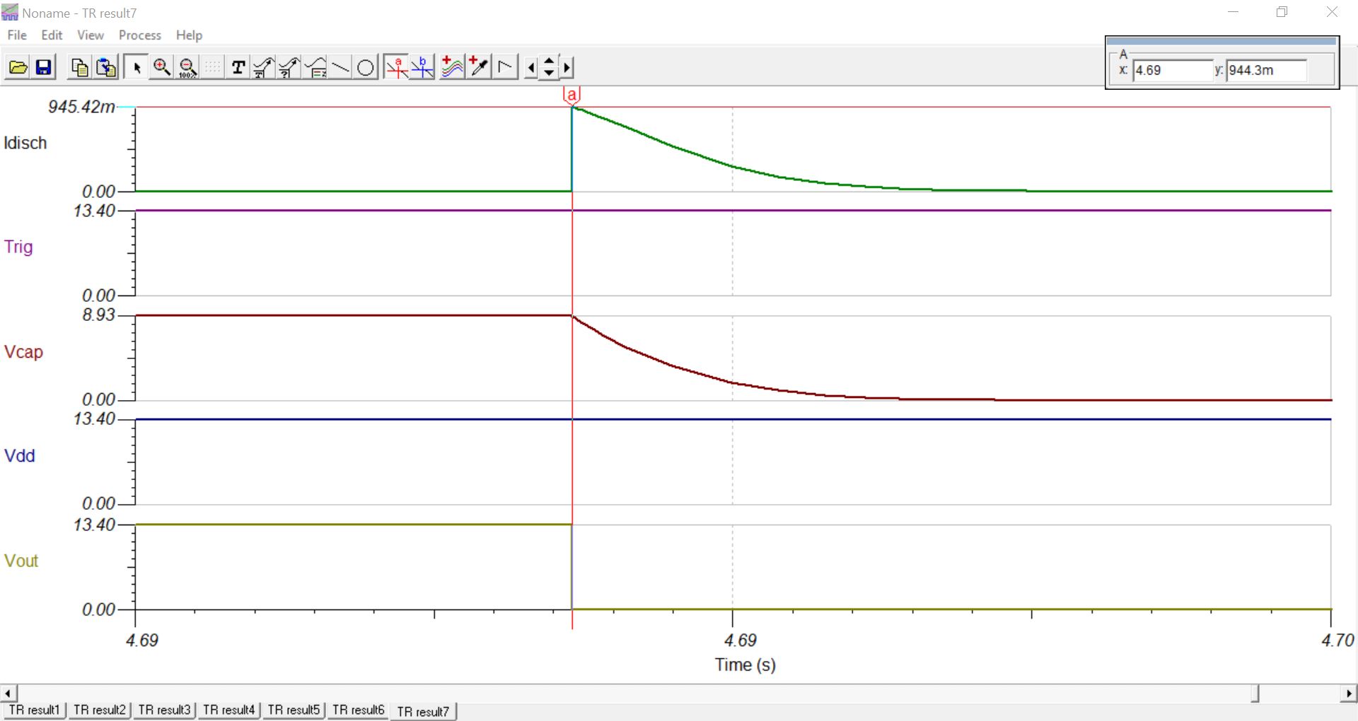
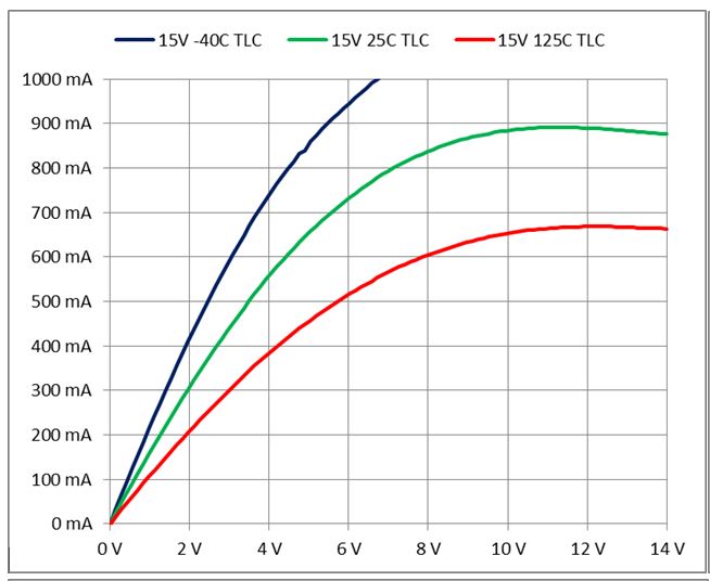
1. How to calculate current flow through transistor when timing capacitor is discharging? 

    The customer wants to confirm current de-rating of transistor when discharging.


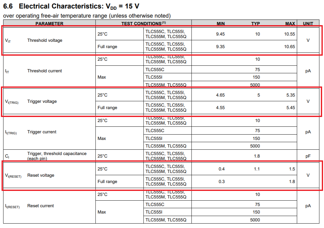
2. The tolerance of trigger level and threshold level (The tolerance of R is also fine)

 The customer wants to confirm the setting time tolerance and the max. voltage that timer start to work. 

I found the sentence below from the datasheet so I think the tolerance would be very small, please let me know if there's a specific value for it. Thanks.

"The resistance of “R" resistors vary with VDD and temperature. The resistors match each other very well across VDD and temperature for a temperature stable control voltage ratio."

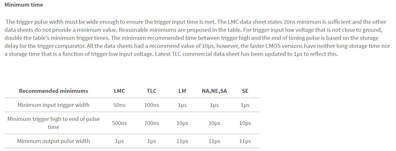
3. Is there restriction for min. width of pulse that input to trigger pin when using as one-shot timer? 

Thanks.

  • Hello,

    1. From the TINA-TI circuit I attached in your previous post, the simulated max discharge current is 944mA. This matches with the expected max discharge current of I=Vcap/R, with Vcap being the initial charge on the capacitor and R being the on resistance of the discharge transistor. Based on the resistor divider on the threshold pin, Vcap will be 8.93V (2*Vdd/3) when the transistor is turned on, and R is probably between 7-9ohms for your supply voltage of 13.4V, as seen in figure 1 of the datasheet.


    2. The datasheet gives max and min ranges for the threshold voltage, trigger voltage, and reset voltage at 25C and full range. 

    There are not specified tolerances for the resistor values themselves and there are no specs for your supply voltage of 13.4V specifically, but the Vdd=2V and Vdd=5V also have min/max values a few hundred mV below/above the ideal value. 


    3. This FAQ on monostable timers answers your third question. 

    Best,

    Katlynne Jones

  • Hi Katlynne

    Thanks for the detailed information.  

    Regarding to inquire 1,

    the customer is wondering if it is possible to acquire value of Ron when not knowing output current since figure.1 in datasheet p.12 only showing Ron when VDD=15V & Io=100mA. 

    Please let me know if you need more parameter information to figure it out.

    Also if it's possible, could you share the TINA-TI file used to simulate the discharge current since i am not quite familiar with it?

    Thanks.

  • Hello,

    I'm attaching the TINA-TI simulation. TLC555_Voh_Vol_13p4V_mono_e2e.TSC

    We have this sample data representing the discharge current vs voltage at a 15V supply. 

    This could help estimate the value of Ron for different drain currents. 

    Best,

    Katlynne Jones

  • Hi Katlynne

    Thanks for the reply and the TINA-TI file. 

    Please let me confirm following with you.

    1. What does "Io" on figure1 in datasheet mean? Is that a constant current source flow into DISCH pin in order to measure Ron ? Since the customer thought that means output current of TLC555, that's the reason for previous question. 

    2. Absolute max. ratings in datasheet showing "Sink, discharge or output" and "Source, output, IO" for current.

    Does it mean that discharge and output pin can sink as much current to 150mA, output and Io can source as much current to 15mA?

    What does "Io" here mean? Does it also mean discharge pin?

    3. Just to make sure, regarding to the sample data you provided above, I think x-axis represents Vcap(Vds for MOSFET), so I can calculate Ron from x-axis(Vds)/y-axis(Id), am i right? 

    Thanks.

  • Hello,

    1. It looks like the data sheet uses Io to refer to the current into or out of the pin that the figure is about. So in the case of Figure 1, this would be current into the DISCH pin. In Figures referring to the output pin, Io means the current on the output pin (such as Figures 5 & 6). 

    2. I believe this Io was left from a previous revision. Previously the discharge pin was not included in this table so Io only referred to the output pin. You should not apply a current of more than 150mA of current to the discharge or output pin. When the discharge transistor discharges the capacitor, we see a current of more than 150mA, this is ok because:

    "The AMR table wants the designer not to exceed the rating. If the device, on it own choice, seems to violate the spec then that is usually acceptable. The data sheet shows the normal example has a capacitor directly on the discharge pin. So the data sheet recommends having this capacitor directly attached and makes no mention about calculating peak current or adding resistance. In this case the AMR limit would not apply to the capacitor."  Please refer to this e2e post

    3. Yes that is correct.

    Best,

    Katlynne Jones

  • Hi Katlynne

    Thanks for your reply.

    Now I am clear for question 1. 

    Regarding to question 2 about discharge current flow into DISCH pin,

    I referred to the article you provided and explained to the customer, 

    but my customer is also worrying about the energy released from external capacitor to transistor. 

    Since larger the external capacitor he uses, larger energy will be released to transistor, so my customer wants to know how much energy the internal transistor can withstand. 

    Since the article below didn't provide such information, it will be helpful if you can help with this.

    Thanks. 

    https://e2e.ti.com/support/clock-and-timing/f/48/t/915841

  • Hello,

    We don't have energy specifications for the internal transistor, as stated in the post I shared with you. I tested the TLC555 using a capacitance vale of 150uF and a supply voltage of 15V. The part functions as expected and the timing was consistent between tests.

    Best,

    Katlynne Jones

  • Hi Katlynne

    Thanks for the information.

    It solves customer's question now. 

    The customer had another question, could you kindly help with this? Thanks.

    He is asking about how much the standard deviation of min. and max. value is predicted (±1,2 or 3σ)for each parameter in Electric Characteristics Table shown in the datasheet?

    Thanks.

  • Hello,

    The typical values in the electrical characteristics table are representative numbers from the time of development and release of the product. Various norms have been followed over the last decades, and we cannot provide assurance of the exact figures of merit used at the time of this product release. I wouldn't consider the maximum and minimum values predicted, as TI does stand behind the maximum and minimum values in the table. We suggests customers design their circuits to perform adequately under all cases, including considerable shifts in typical values.

    Best,

    Katlynne Jones