Replies: 12
Views: 161
Part Number: LMK04828
Hello
Now I try to "direct sysref mode" but It doesnt work (no output and signal fixed to LOW . input SYNC signal is High.)
My Configuration is as below. (SYSREF signal is conected to Clkin0 )
0x143 0x10 SYNC_MODE
0x139 0x04 SYSREF_MUX,SYSREF CLKin0_MUX
0x147 0x18 CLKin0_OUT_MUX
0x104 0x20 SDCLKoutY_DDLY
0x140 0x07 SYSREF_DDLY_PD,PLSR,PD
0x106 0x30 SDCLKoutY_PD
0x107 0x55 SDCLKoutY_FMT
Would you please tell me something wrong point?
Takeshi
Hello Takeshi-san,
Do you have a full .tcs file or programming I could load? I could confirm tomorrow.
73,Timothy
____________________________________________________________________________________
More information Clock and Timing System products: http://www.ti.com/clock-and-timing/overview.html
In reply to Timothy T:
Hello Timothy
I dont have tcs file . Full programming is below.
0X0000 0X00800X0000 0X00000X0002 0X00000X0100 0X00040X0101 0X00560X0103 0X00000X0104 0X00200X0105 0X00000X0106 0X00300X0107 0X00550X0108 0X000A0X0109 0X00560X010B 0X00000X010C 0X00200X010D 0X00000X010E 0X00F10X010F 0X00110X0110 0X00040X0111 0X00560X0113 0X00000X0114 0X00200X0115 0X00000X0116 0X00F00X0117 0X00550X0118 0X00100X0119 0X00550X011B 0X00000X011C 0X00200X011D 0X00000X011E 0X00F00X011F 0X00110X0120 0X000A0X0121 0X00890X0123 0X00000X0124 0X00200X0125 0X00000X0126 0X00F00X0127 0X00110X0128 0X000A0X0129 0X00560X012B 0X00000X012C 0X00200X012D 0X00000X012E 0X00F00X012F 0X00110X0130 0X00040X0131 0X00890X0133 0X00000X0134 0X00200X0135 0X00000X0136 0X00F00X0137 0X00550X0138 0X00050X0139 0X00040X013A 0X00050X013B 0X00000X013C 0X00000X013D 0X00080X013E 0X00000X013F 0X00000X0140 0X00070X0141 0X00000X0142 0X00000X0143 0X00100X0144 0X00000X0145 0X007F0X0146 0X00080X0147 0X00180X0148 0X00330X0149 0X00330X014A 0X00020X014B 0X00020X014C 0X00000X014D 0X00000X014E 0X00000X014F 0X007F0X0150 0X00000X0151 0X00020X0152 0X00000X0153 0X00000X0154 0X00050X0155 0X00000X0156 0X00050X0157 0X00000X0158 0X00960X0159 0X00000X015A 0X00010X015B 0X00DF0X015C 0X00080X015D 0X00990X015E 0X00000X015F 0X000B0X0160 0X00000X0161 0X00010X0162 0X00A00X0163 0X00000X0164 0X00000X0165 0X000C0X0171 0X00AA0X0172 0X00020X017C 0X00150X017D 0X00330X0166 0X00000X0167 0X00000X0168 0X00100X0169 0X00590X016A 0X00200X016B 0X00000X016C 0X00000X016D 0X00000X016E 0X00130X0173 0X0000
In reply to user5983069:
Thank-you for the full programming. I was able to confirm operation. The settings you are using appear correct.
Can you please check that pin 5, the reset pin is in a LOW state. If the device is held in reset, then your programming wouldn't take effect.
- Have you been able to confirm programming? You could do this by toggling the POWERDOWN bit R2[0] to 1, if device current reduces then programming is working. You could also toggle the polarity of the output PLL1_LD or PLL2_LD pin by using the PLLx_LD_TYPE to toggle to an output inverted setting to confirm those pins respond to the inversion.
If further investigation is needed, can you share your schematic? What is the schematic of your input to CLKin0? What type of signal are you providing to CLKin0?
I checked that pin 5 is in a LOW state. And another 614MHz CLK is outputted so no reset state.
I input LVDS(output from LMK04803 and 100Ω terminated and AC coupled) signal to CLKin0 . input voltage Vpp is 844mV measured at Device pin.
Frequency is 1.92MHz.
Sorry I checked output SYSREF signal again and it was outputted .
But output frequency is 10 Hz,1KHz,,,not stable..
When I stopped SYSREF Which is inputed Clkin0 ,still SYSREF is outputted .
so it doesnt works.
.
How many boards have you tested this on?
Can you confirm 3.3 V at each Vcc pin?
I checked 2 devices and confirmed that all Vcc pin is3.3V.
Can you share the schematic? Particularly the CLKin0 section?
You mention getting getting some output when no CLKin0 is driven. I presume you are AC coupling and there is no 100 ohm resistor on the IC side of the CLKin0? Change the input type to (CLKin0_TYPE = 1: MOS). This is register 0x146[0] = 1.
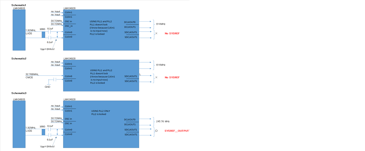
I added schematics. I changed input signal and CLOCKin0_TYPE =1,but sysref was not outputted.(see. schematic 2)
In Schematic.3 I could output SYSREF.
When I didnt input SYSREF signal inSchematic 3 CLKin0 pin,sysref was not outputted ,so Direct sysref distribution function works.
The diffrence between Schematic 1 and 3 is using PLL1 or not.
Are there some conditions to stop output SYSREF?? for example if pll1 is unlocked,then stopping output sysref or etc...?
I add configuration for Schematic3 below.
0 0X0000 0X00800 0X0000 0X00000 0X0002 0X00000 0X0100 0X000A0 0X0101 0X00230 0X0103 0X00000 0X0104 0X00200 0X0105 0X00000 0X0106 0X00300 0X0107 0X00110 0X0108 0X00040 0X0109 0X00230 0X010B 0X00000 0X010C 0X00200 0X010D 0X00000 0X010E 0X00F00 0X010F 0X00550 0X0110 0X00040 0X0111 0X00230 0X0113 0X00000 0X0114 0X00200 0X0115 0X00000 0X0116 0X00F00 0X0117 0X00550 0X0118 0X000A0 0X0119 0X00230 0X011B 0X00000 0X011C 0X00200 0X011D 0X00000 0X011E 0X00F00 0X011F 0X00110 0X0120 0X00080 0X0121 0X00450 0X0123 0X00000 0X0124 0X00200 0X0125 0X00000 0X0126 0X00F00 0X0127 0X00110 0X0128 0X00040 0X0129 0X00450 0X012B 0X00000 0X012C 0X00200 0X012D 0X00000 0X012E 0X00F00 0X012F 0X00550 0X0130 0X000A0 0X0131 0X00450 0X0133 0X00000 0X0134 0X00200 0X0135 0X00000 0X0136 0X00F00 0X0137 0X00110 0X0138 0X00050 0X0139 0X00040 0X013A 0X00050 0X013B 0X00000 0X013C 0X00000 0X013D 0X00080 0X013E 0X00000 0X013F 0X00000 0X0140 0X00070 0X0141 0X00000 0X0142 0X00000 0X0143 0X00100 0X0144 0X00000 0X0145 0X007F0 0X0146 0X00080 0X0147 0X00180 0X0148 0X00330 0X0149 0X00330 0X014A 0X00020 0X014B 0X00020 0X014C 0X00000 0X014D 0X00000 0X014E 0X00000 0X014F 0X007F0 0X0150 0X00000 0X0151 0X00020 0X0152 0X00000 0X0153 0X00000 0X0154 0X00050 0X0155 0X00000 0X0156 0X00050 0X0157 0X00000 0X0158 0X00960 0X0159 0X00000 0X015A 0X00010 0X015B 0X00DF0 0X015C 0X00080 0X015D 0X00990 0X015E 0X00000 0X015F 0X000B0 0X0160 0X00000 0X0161 0X00010 0X0162 0X00A00 0X0163 0X00000 0X0164 0X00000 0X0165 0X000C0 0X0171 0X00AA0 0X0172 0X00020 0X017C 0X00150 0X017D 0X00330 0X0166 0X00000 0X0167 0X00000 0X0168 0X00100 0X0169 0X00590 0X016A 0X00200 0X016B 0X00000 0X016C 0X00000 0X016D 0X00000 0X016E 0X00130 0X0173 0X0000
user5983069 I added schematics. I changed input signal and CLOCKin0_TYPE =1,but sysref was not outputted.(see. schematic 2)
Note, it is acceptable to use the MOS mode with Schematic 1. MOS mode has a larger (50 mV) threshold wwhich will prevent noise from oscillating the input buffer when no input is present. This is important given the AC coupling to CLKin0. It is recommended to use MOS mode for AC coupled inputs which may be turned off. (As for LOS detect note).
user5983069In Schematic.3 I could output SYSREF.
When SYSREF was output, this was a well behaved 1.92 MHz signal? I am concerned your capacitors may be too small.
There is no difference in your schematic 1 vs. schematic 3 which should change behavior. PLL lock should not have an impact. In my test neither PLL1 or PLL2 is locked.
user5983069When I didnt input SYSREF signal inSchematic 3 CLKin0 pin,sysref was not outputted ,so Direct sysref distribution function works.
user5983069I add configuration for Schematic3 below.
It appears this config is using bipolar input. If you do not use MOS mode and stop the signal, there is a risk that it may output noise.
user5983069 The diffrence between Schematic 1 and 3 is using PLL1 or not. Are there some conditions to stop output SYSREF?? for example if pll1 is unlocked,then stopping output sysref or etc...?
There are no conditions that would stop output of SYSREF. There are bits to enable sync if PLL1 or PLL2 is unlocked, but SYSREF would not be impacted by these SYNC.
--
One suggestion I have is to use a higher value capacitor for CLKin0 AC coupling. 0.1 uF is quite small for 1.92 MHz.