This thread has been locked.

If you have a related question, please click the "Ask a related question" button in the top right corner. The newly created question will be automatically linked to this question.

LMK04828: Distribution mode phase noise

Part Number: LMK04828
Other Parts Discussed in Thread: DAC37J82

Hi Liam

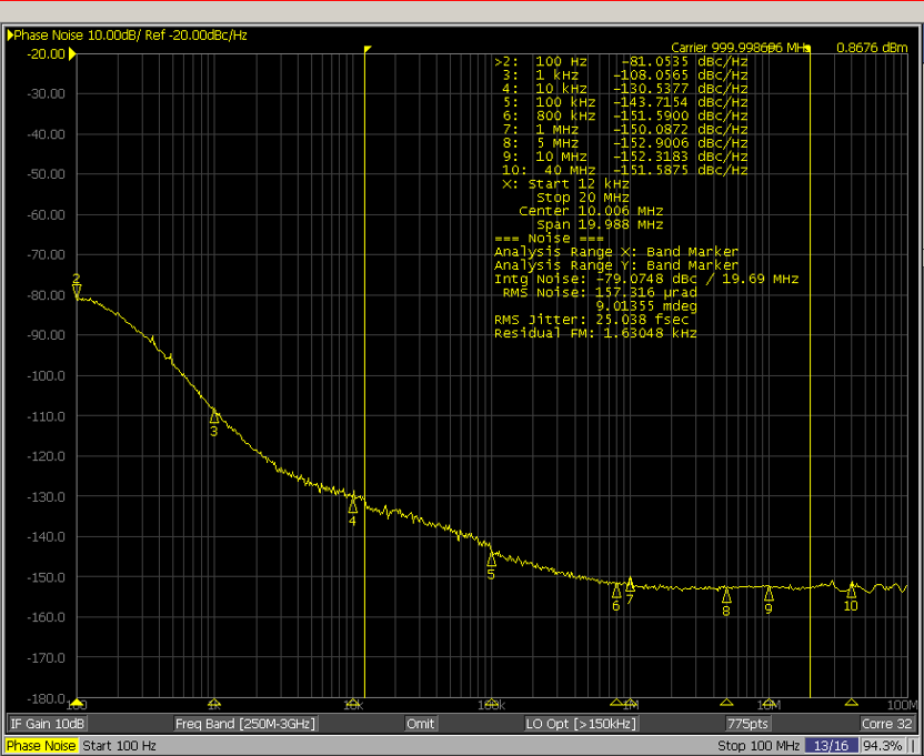
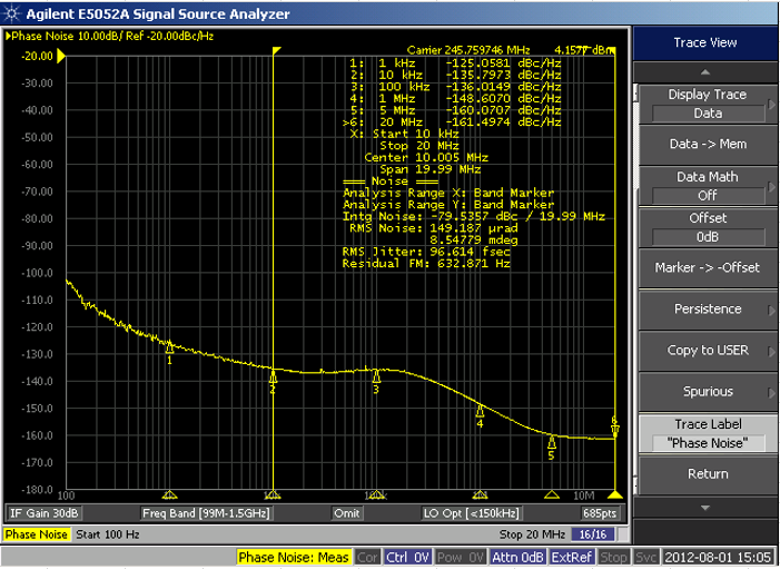
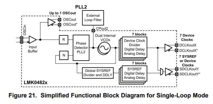
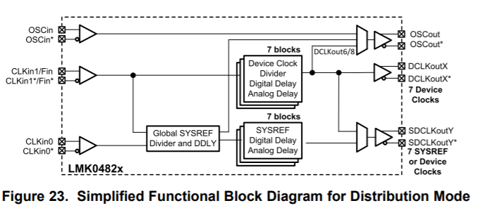
We want to use the LMK04828 in distribution mode (no PLL) with with following parameters:

Input clock = 800 MHz

Output clock1 = 800 MHz

Output clock2 = 200 MHz

Do you perhaps have phase noise diagrams for the above scenario?

This is for use with the Ti DAC37J82 device .

Please advise

Kind regards

Piet

  • Hello Piet,

    Below is a phase noise plot for a 1000 MHz output when the LMK04828 is in distribution mode and the input frequency is 1000 MHz. This data is the closest data we have to your scenario.

    The phase noise plot for your 800 MHz output should follow a similar trend to the plot above.

    Regards,

    Kia Rahbar

  • Hi Kia

    Thanks for the feedback and graph. 

    Do you perhaps also have a graph of a ~ 200 MHz output with an 800 MHz (or 1000 MHz) input.

    Thanks

    Piet

  • Hi Kia

    Related to the above, I note that the maximum input frequency on ClkIn is 750 MHz and 3100 MHz for Fin.

    • What is the limiting factor of the input frequency in Single/Dual PLL modes?
    • Is an 800 MHz input frequency at all possible in Single/Dual PLL modes?

    Kind regards

    Piet

  • Hello Piet,

    1. Unfortunately, we do not have any plots of a ~200 MHz output for distribution mode.

    2. The limiting factor of the input frequency is the output buffer. Each output format will have a different output buffer to produce different signal swings. Up until the output divider (through the channel divider), the device will be able to generate the higher frequencies. Once the signal hits the output buffers, the output format (LVDS, LVPECL, LVCMOS) will limit the frequency. 

    3. A 800 MHz input frequency would not be possible in single/dual PLL modes. The maximum input frequency in single PLL mode would be 500 MHz and the maximum input frequency in dual PLL mode would be 750 MHz.

    Regards,

    Kia Rahbar

  • Hi Kia

    Thanks for the reply.

    1. Do you perhaps have a more commonly used 245 MHz diagram for distribution mode, or another frequency close to 200 MHz?

    2. I'm not 100% clear on this. Are the same output pins not used in Distribution or PLL mode, with a max output frequency of 3.1 GHz for LVPECL?

    3. Does the input clock pin mode (mux selection) not determine the maximum frequency?
         i.e. 3100 MHz for Fin, 750 MHz for fFBClkin, CLKin_0/1/2 and 500 MHz for OSCin ?

    Please advise

    Kind regards

    Piet

  • Hello Piet,

    1. The best I can provide you is a phase noise plot of 245 MHz for single-loop mode (shown below).

    2/3. In single-loop mode, the only input is OSCin as shown below.

    Since this is the only input, the input frequency is limited by the OSCin frequency range (shown below).

    In dual-loop mode, the only input is CLKin as shown below.

    Since this is the only input, the input frequency is limited by the CLKin frequency range (shown below).

    In distribution mode, there are three possible inputs: CLKin, Fin, and OSCin (shown below).

    The maximum input frequency for distribution mode is determined based off which input is used. For a CLKin input, the maximum input frequency would be 750 MHz as shown above. For a OSCin input, the maximum input frequency would be 500 MHz as shown above. For a Fin input, the maximum input frequency is limited by the Fin frequency range shown below.

    To sum it up, the input type limits the maximum input frequency and a 800 MHz input is only possible when the device is used in distribution mode and the 800 MHz signal is feed into the Fin pin.

    Regards,

    Kia Rahbar

  • Hi Kia

    Thanks for the information.

    Does this mean that the input frequency can be higher than 750 MHz in single-PLL mode when using the CLKin1/Fin input, since Fin and CLKin1 is the same physical pins?

    Kind regards

    Piet

  • Hello Piet,

    Single PLL mode has OSCin as an input (as shown in figure 21 in my last post). The maximum input frequency for OSCin is 500 MHz, so in single PLL mode the input frequency cannot be greater than 500 MHz.

    Distribution mode is the only mode where the input frequency higher than 750 MHz can be used. Distribution mode is the only mode that uses Fin as an input.

    Regards,

    Kia Rahbar

  • Hi Kia

    Sorry, my mistake.

    I meant dual-loop mode (Fig. 18), which uses Fin input.

    From the pin list, FIn and Clkin1 are the same pins, see below.

    Is there a functional/performance difference, depending on which mode the CLKin1 pin is used, .e.g Distribution mode or PLL mode?

    Kind regards

    Piet

  • Hello Piet,

    In distribution mode, the input frequency is feed into a clock divider and then outputted from the device. Since we are only dividing the frequency in distribution mode, a much higher input frequency can be used. This is why we can use the Fin limit of 3.1 GHz.

    In dual-loop mode, the input frequency is feed into a PLL. If a large frequency is feed into the PLL, the PLL will not be able to lock to that input frequency (due to the limitations of the phase detector frequency and the VCO frequency). This is why we use the CLKin limit of 750 MHz.

    Regards,

    Kia Rahbar

  • Hi Kia

    Thanks for the feedback.

    Kind regards

    Piet