Replies: 10
Views: 110
Part Number: LMK04828
Hi,
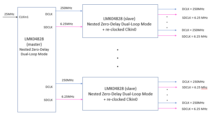
i am planning to set the LMK04828 in nested ZDM mode + reclock clkin0 for sysref.
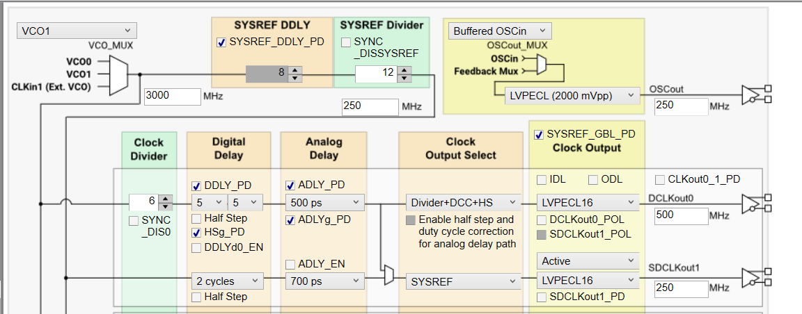
Below in my frequency plans:
Dclk = 250MHz
SDclk = 6.25MHz
Clkin1 = 250MHz
clkin0 = 6.25MHz
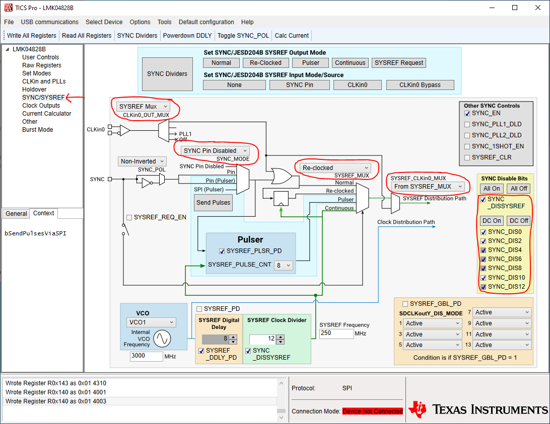
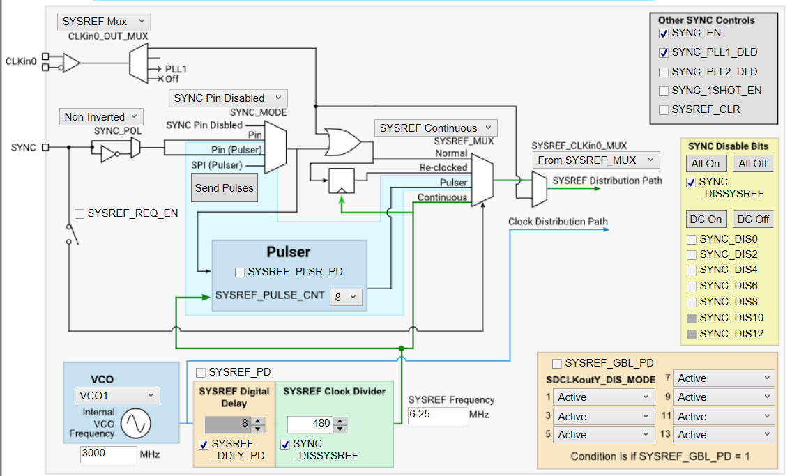
i set the internal SYSREF divider to output 250 MHz and use it as ZDM feedback for PLL1. To get the SDCLK, i wanted to configure the SYSREF muxes to forward CLKin0 to SDCLKoutY as the figure attached below. however, i am not able to do so in TICS. the source of SDCLKout is from either SYSREF divider or DCLK.
Can you advise how to configure correctly?
Thanks.
i attached the images again.
In reply to KGY:
Hi KGY,
On the SYNC/SYSREF page, set the following controls:
Regards,
Derek Payne
Texas Instruments
In reply to Derek Payne:
Hi Derek,
Thanks for the prompt reply.
after the settings on the "SYNC/SYSREF" page, what settings should i do on the "Clock Outputs" page to get the clkin0 forwarded to the SDCLKoutY?
Based on the image you provided, you already have SDCLKout1 configured correctly to distribute the re-clocked signal from CLKin0 (SDCLKoutY_MUX set to SYSREF, SDCLKoutY_PD=0). You can use this as a template for setting the other SDCLKoutY outputs.
if my overall clock design is as attached and the slave is configured as above (ZDM with reclocked clkin0), does my design ensure that all the slave LMK04828s' outputs will be synchronized and have the rising edge at the same time?
I ended up with a lot to say, but much of it is supplementary. My core answer is the three paragraphs below; the remainder are notes that are covered in the datasheet, but which are helpful to have summarized in one location.
The design as drawn, with the configuration in your TICS Pro screenshots and description, should ensure that the SYSREF edge of each slave LMK is synchronous with the DCLK output of each master LMK. It looks like the master device is generating the 6.25MHz SYSREF, and since the reference of the master device is 25MHz I assume the zero-delay PLL1 feedback is the SYSREF and the phase detector rate is also 6.25MHz (or an integer divide of 6.25MHz).
In practice, you will need to SYNC the dividers to ensure that every slave DCLK is aligned after programming, because programming the divider value effectively randomizes the divider phase. The timing and source of the SYNC are not critical for the master device. It is only important that all the master LMK DCLKs are aligned with each other and the SDCLKs are at least slightly delayed from the DCLK edges, by setting the appropriate digital delays before the SYNC procedure. For the slave devices, as long as the SYNC is retimed to the slave LMK SYSREF divider (which is in-phase with the master's DCLKs and therefore simultaneous across all slave LMKs), the SYNC timing and source are not critical. As long as the digital delay values on the slave devices are all the same, the phase of all slave devices should agree after synchronization.
Since all devices are in nested zero delay mode, I think the easiest way to ensure all devices are synchronized is to set SYNC_PLL1_DLD on the SYNC/SYSREF page during programming, set SYNC_DISx = 0 for all DCLK dividers (SYNC_DISSYSREF=1 still), lock the devices, and then set SYNC_DISx = 1 again. As the master LMK locks, SYNC from PLL1_DLD will de-assert, and all the master DCLKs will be synchronized. Setting SYNC_DISx = 1 at the end ensures the DCLK dividers are not needlessly reset by the SYSREF divider. After the master locks, the 250MHz DCLKs will begin switching, and the slave devices will begin to lock. As the slave LMKs lock, SYNC from PLL1_DLD will de-assert, and the SYNC signal of all the slave DCLKs will be synchronized to the master LMK 250MHz edge through the SYSREF divider re-clock. Setting SYNC_DISx = 1 at the end ensures the slave DCLK dividers are not needlessly reset by the re-clocked CLKin0 signal. After each slave device is locked, its 250MHz DCLKs will begin to switch. After each device is locked, SYNC_PLL1_DLD can be set to 0 to prevent unwanted signals to the SYSREF_MUX in the event of a temporary loss-of-lock. Note that after synchronization, the synchronization of all devices can persist through any device temporarily losing and re-acquiring lock, because of the zero-delay and because GCD(inputs, outputs) is always equal to the feedback frequency.
Additional notes that may be useful:
Thanks for the great information.
I have a few more questions.
1. i wanted to get the best jitter at the slave outputs, so i have designed the slave to be in nested zero-delay dual-loop too. will there be difference in jitter performance for the below 2 cases?
nested zero-delay dual-loop for both master and slave:
master FPD1 = 6.25MHz, master FPD2 = 125MHz, slave FPD1 = 25MHz, slave FPD2 = 125MHz
master in nested zero-delay dual-loop, slave in PLL2-only zero-delay mode:
master FPD1 = 6.25MHz, master FPD2 = 125MHz, slave FPD2 = 125MHz
2. On the master LMK, for the synchronization, is the sequence below correct?
a) set SYNC_DISSYSREF=0 to enable synchronization of the dividers
b) set SYSREF_MUX to normal and toggle SYNC_POL
c) set SYNC_DISSYSREF=1
d) set SYSREF_MUX to continuous
Hello KGY,
Thanks, I have clearer understanding now.
A last question, is the configuration and the programming sequence(mentioned above) the same if i switch to LMK04832?
The register programming is somewhat different between LMK04828 and LMK04832. The two devices are p2p compatible, but they do not share identical functionality. A comprehensive overview of the register map and functional changes between the devices is attached.
LMK04828 to LMK04832 Migration Guide.pdf