This thread has been locked.

If you have a related question, please click the "Ask a related question" button in the top right corner. The newly created question will be automatically linked to this question.

Clock buffer / mux / jitter cleaner part selection

Other Parts Discussed in Thread: CDCE6214

Hello,

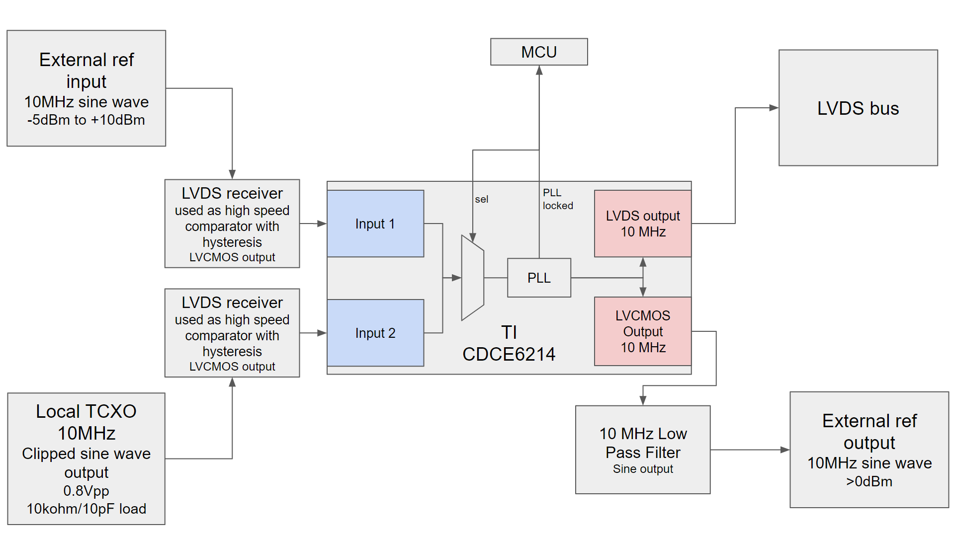
I am working on a device which takes as an input an external 10 MHz clock ref or a local oscillator. This device should generate a 10MHz sine wave output as well as an LVDS clock.

Could you please recommend a part or parts that can correspond to the following block diagram please?

Thank you in advance,

Victor

  • Hello Victor,

    Could you specify the jitter cleaning specifications for this device?

    We do not offer Jitter Cleaners with a sinewave output and therefore require a 2-chip solution if we could not meet jitter requirements utilizing a Clock Generator.

    Thank you for the additional input.

  • Hello Aaron,

    Yes, we are using FPGAs on the LVDS bus, and we would need 6ps RMS jitter on this LVDS bus.

    I have updated the diagram with my last thoughts.

    The idea is to convert both sine input and clipped sine input to LVCMOS signals using LVDS receivers with 100mV hysteresis. I have no idea what phase noise or jitter I can expect from this conversion. What do you think?

    Then we would use CDCE6214 with a low LPF setting to clean the clock.

    The first LVDS output would be used as is, then the LVCMOS output would be filtered to keep only the fundamental of the signal. Do you think it is a good way to generate a 10 MHz sine ref clock, or should I use another topology to achieve this ?

    Many thanks,

    Victor

  • Hello Victor,

    Please make note that the CDCE6214 general input levels 0.2xVdd to 0.8xVdd, at 10dBm (2V) this will not be enough to operate at 3.3V and this will be marginal at 2.5V.

    Also note the recommended crystal requirements within section 7.8 of the Datasheet.

    If CDCE6214 is utilized as 'Jitter Cleaner' the RMS Phase Jitter expected out could be as high as 2.1ps if the PLL was utilized. Since frequency is not changing this jitter should be less. The LVDS bus should have no issue with jitter as the worst case output will be able to meet a spec of 6ps RMS jitter.

    Unfortunately after further research we don't offer any devices with capability of converting typical square waves to sine waves. The best option is to use filtering as you have have mentioned either 1st or 2nd order should be okay, if additional information is required please let me know. 

  • Hello Aaron,

    Thanks for your answer.

    I do not plan to use the crystal input mode. I would use only the 2 single ended inputs of the CDCE6214 connected to LVDS to CMOS converters that would act as high speed comparator.

    One last thing, would hysteresis be desirable in this sine to digital conversion? I would guess it won't hurt, given the slow slew rate of the incoming signal.

  • Hello Victor,

    I'm assuming hysteresis is just meaning the centering of your signal input at VDD/2, this would require checking with your device input requirements.