This thread has been locked.

If you have a related question, please click the "Ask a related question" button in the top right corner. The newly created question will be automatically linked to this question.

LMK04906: OSCout/CLKout Phase Noise in Datasheet/Simulation Tool measured Single-Ended or Differential?

Part Number: LMK04906
Other Parts Discussed in Thread: LMX2492, LMK04816, LP5912

Hi,

The LMK04906 datasheet gives a phase noise plot on page 108 comparing OSCout/CLKout VCXO and VCO phase noise performance. Is this measurement taken as described on page 91 (Figure 34)? I.e. is this figure measured single-ended or differentially (using an external balun)?

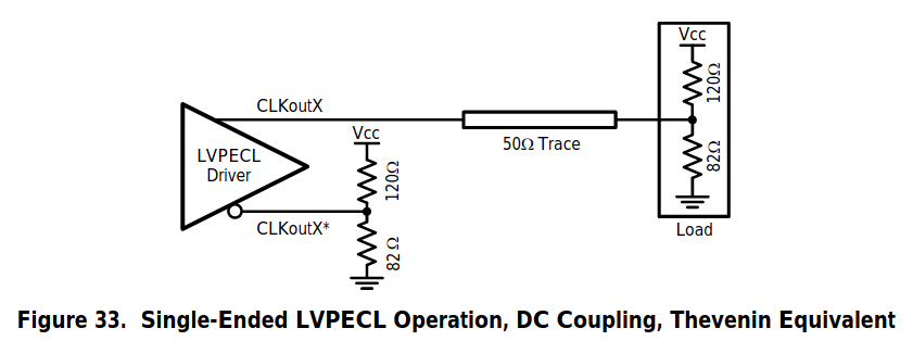
We designed the LMK04906 into a product but we cannot achieve the same noise floor performance of the OSCout/CLKout output as given in the datasheet. However we are using the LVPECL OSCout0 output as two single-ended outputs as shown in Figure 33 (page 91). We are now questioning whether we can actually do something about it.

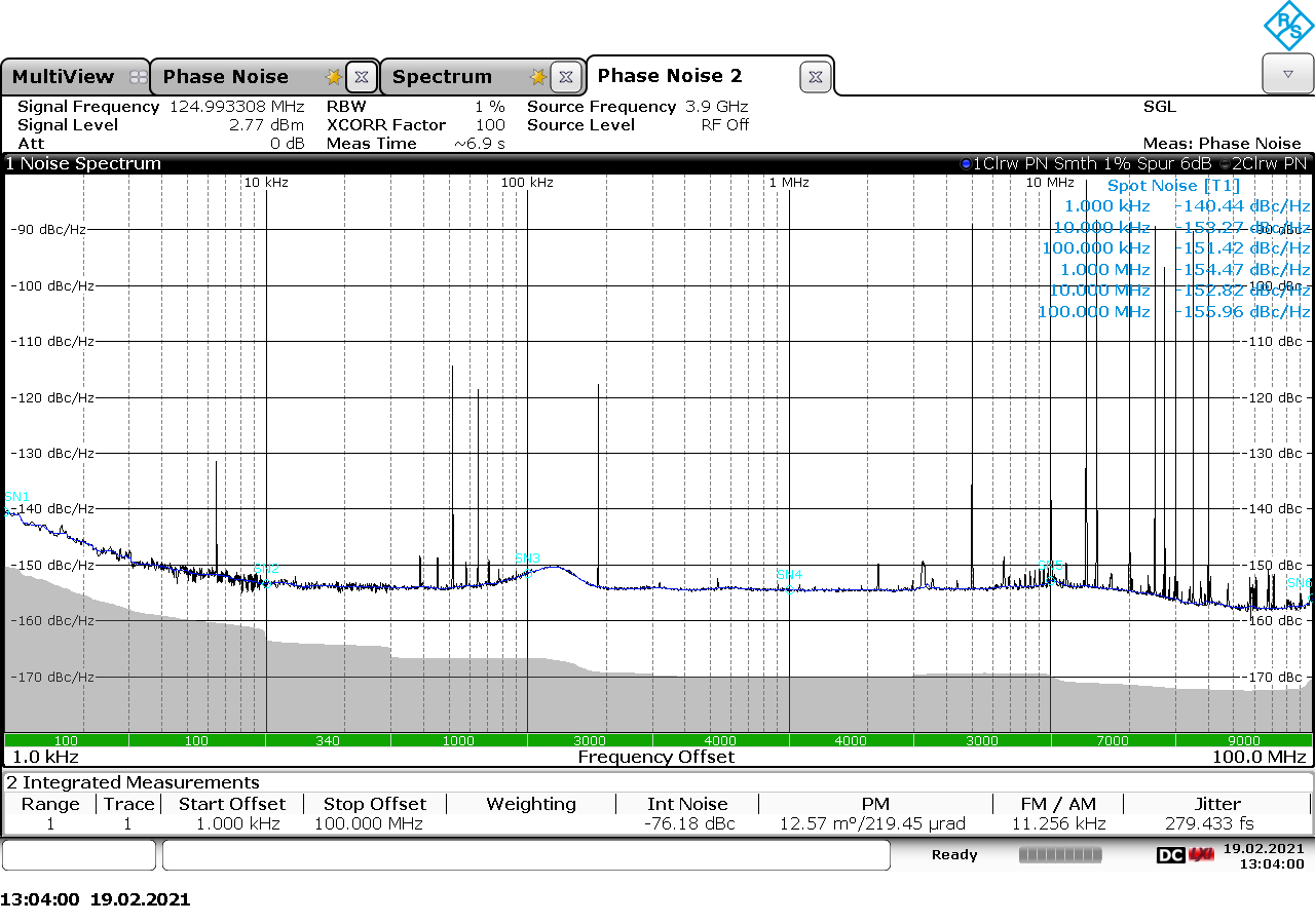
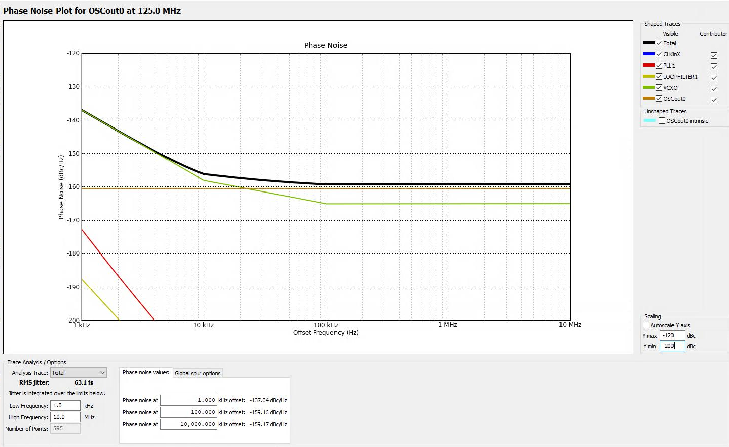
We are able to reach about -150dBc/Hz as the noise floor. The reference clock is a 125 MHz Ultra Low-Noise Crystal Oscillator with LVCMOS Output (1kHz: -137dBc/Hz, 10kHz: -158dBc/Hz, 100kHz: -167dBc/Hz, floor: -169dBc/Hz). According to the simulation we should reach close to -159dBc/Hz on the OSCout0 output with LVPECL standard and divider bypassed.

If the simulated figure is realistic in our single-ended scenario, any hints on what we could try to reduce the noise floor? Which supply voltage pins can raise the noise floor of the chip?

Best Regards and Thank you in advance

  • Hello Simon,

    I wouldn't expect the balun to be the issue for such a large change in noise floor.

    Are those numbers for your low noise oscillator measured in-circuit or a spec?  Would it be possible to measure in circuit the performance of the oscillator?  If something happened to make that performance degrade before it hit the input buffer, you wouldn't get it back of course.

    Are you using a voltage divider on the OSCin input to reduce the LVCMOS output voltage to between 0.2 Vpp and 2.4 Vpp as per Voscin specification?

    Are you using the same resistor values as illustrated on figure 33?

    73,
    Timothy

  • Hi Timothy,

    For clarification, we do not use a balun in our application. We split the differential LVPECL in two (180° shifted) single-ended LVPECL signals that are routed to two other ICs (LMX2492, ADF41513) similar to Figure 33 of the datasheet.

    What I originally meant is, whether characterization of the noise-floor given in Figure 38 in the datasheet was carried out by using the differential LVPECL (with a balun between the LMK04906 and the signal analyzer) or single-ended signal according to Figure 34. Of course by using the output as single-ended the output signal now additionally contains common-mode noise, which is usually suppressed when using the LVPECL output differentially. My question was, whether this common-mode noise can be the cause of the increase in the noise floor.

    The phase-noise numbers given from me above are measured in-circuit, however clock output and tune voltage disconnected from the LMK04906 currently. So in theory the output of the VCXO should be quite pure, which already took some time for debugging its power supply, but that is another story.

    Interesting that you mention the voltage divider and the V_OSCin input range. Have you seen my other thread? https://e2e.ti.com/support/clock-and-timing/f/48/p/975043/3602583

    We are currently using just a DC-Block and no voltage divider as shown in the LMK04906BEVM, however we are questioning whether this is the right way to go, since as you say, this way we are not complying to the maximum input voltage as given in the Electrical Characteristics table. Do you think that this could be an issue? Also, is the value of the DC-Block capacitor important? We are using 10nF for a 125MHz LVCMOS signal but I am unsure whether this increases the noise floor of the LMK04906 input stage below the cutoff frequency of the DC-block formed with the LMK04906 input impedance.

    This will probably be the next thing we are going to try.

    Thanks for your reply and best regards

    Simon

  • Hello Simon,

    Simon Kueppers said:
    Have you seen my other thread?

    I have not see the other thread.  I just glanced over it.  The CLKin inputs do have  MOS input mode which can be used with direct CMOS input.  The OSCin does not, so that is not 100% correct.  Yes, use the LMK04816 input termination.

    Simon Kueppers said:
    What I originally meant is, whether characterization of the noise-floor given in Figure 38 in the datasheet was carried out by using the differential LVPECL (with a balun between the LMK04906 and the signal analyzer) or single-ended signal according to Figure 34.

    I'm not sure the method used in this measurement.

    However, the stated noise floor of your input (-169 dBc/Hz) is less than the noise floor given in the example (-165 dBc/Hz), and the noise you measure (-150 dBc/Hz) is approximately 10 dB greater than the noise floor illustrated in the image.  I wouldn't expect the different in SE to Diff would create such a difference in noise floor measurement.

    Simon Kueppers said:
    this way we are not complying to the maximum input voltage as given in the Electrical Characteristics table. Do you think that this could be an issue?


    I think this could be an issue.

    Simon Kueppers said:
    Also, is the value of the DC-Block capacitor important? We are using 10nF for a 125MHz LVCMOS signal but I am unsure whether this increases the noise floor of the LMK04906 input stage below the cutoff frequency of the DC-block formed with the LMK04906 input impedance.


    I don't think this capacitor value is an issue.

    Let me know what happens with the reduced input voltage.

    73,
    Timothy

  • Hi Simon,

    Do you still require support for this issue? If we don't hear from you, I'll mark it resolved.

    Regards,

  • Hi Derek,

    Thanks for asking. I have not yet been able to further debug the problem above due to the strong weather in europe lately.

    Will be back to measuring at the end of the week.

    Best Regards

  • I have now measured the reference VCXO in-circuit and already did a lot of debugging to improve the in-circuit phase noise of it.

    I was able to get very close to the VCXO spec of

    1 kHz: -137 dBc/Hz
    10 kHz: -158 dBc/Hz
    100 kHz: -167 dBc/Hz
    1 MHz: - 169 dBc/Hz

    There is however still a single peak from a DC/DC converter at around 400 kHz left (and moving around) which we hopefully can eliminate in a next Hardware Revision (as well as the spurs above 3 MHz).

    The VCXO was again connected to the LMK04906 using the voltage divider circuit (100R/51R) and 100nF DC-blocking caps from LMK04816 EVM. I then measured the OSCout LVPECL output exactly as shown in Fig. 34 (above and in the LMK04906 datasheet). Vtune of the VCXO is open (bypassed to ground with 100nF) and not connected to the LMK04906, thus fully open-loop. This is the result:

    The peak is obviously still present (has since shifted to around 130 kHz) and some lower frequency spurs are visible which however could stem from the measurement setup (have to confirm).

    In this measurement we could achieve an OSCout noise floor of around 154 dBc/Hz which I think is still missing a few decibels compared to what the datasheet and the Clock Design Tool suggests. I used very conservative values for the VCXO phase noise (around -165 dBc/Hz noise floor) to get a feel for how it influences the OSCout output. However even with this setting, I should still be able to get to around -158 dBc/Hz noise floor according to the simulation.

    I am wondering what could be the source of such an increased noise floor.. I was thinking that maybe the UWIRE lines connected to an FPGA (with grounded pins) could be the issue, but I think that the FPGA ground noise should be rather peaky and not flat.

    I was thinking that the difference in increased noise floor is awfully close to the -3dB of lost SNR when going from differential LVPECL to single-ended LVPECL (as it was measured here), that is why I asked above if the simulated curves and datasheet curves are recorded differentially (e.g. using some kind of external BALUN). EDIT: I was able to get my hands on a 180° hybrid suitable for 125 MHz on short notice and tried this theory. It seems you are right, the difference between differential and single-ended was barely noticable.

    The power supply is closely designed to the EVM, however we are using a LP5912 LDO supplied from a filtered DC/DC converter module to power the LMK04906 chip.

    The 100R/51R voltage divider divides the 3.3V LVCMOS voltage signal swing down to 1.1Vpp. Is this maybe not enough to get high enough above the OSCin noise level? EDIT: I tried swapping the voltage divider to 51R series 100R shunt and the noise floor decreased consistently by about 1.0 to 1.5 dB. I replaced the voltage divider by a short (LMK04906-EVM style) and noise floor level was back up. I am starting to suspect the input slew-rate of the VCXO might not be enough.

    Any idea where we could start poking around to see what makes a difference?

    EDIT: I was further playing around with the OSCin circuitry and by using the following circuit, I could now reach 157 dBc/Hz

    VCXO-> 10nF Series -> 33R Series/100R Shunt -> 10nF Series -> OSCin*, Other OSCin connected to ground via 10nF.

    Still missing 2 dB unfortunately, but I will leave it this way now although we could really use those 2 dB :-)

    I converted the -160dBc/Hz and an approx. 3dBm (50 ohms) to approx. 100nV/sqrtHz. I am unsure of the power supply rejection ratio of the OSCin buffer, but this is easily in the range of the power supply noise at node Vcc7. I noticed that the LMK04816 uses a 1000R (!) ferrite to the VccPLLPlane which filters the noise above around 100 kHz (just after peaking for a few dB, which is visible in the measured spectrum even). So in my mind it might be possible to R-C filter the Vcc7 pin for a better noise response.

  • Hello Simon,

    Simon Kueppers said:
    In this measurement we could achieve an OSCout noise floor of around 154 dBc/Hz which I think is still missing a few decibels compared to what the datasheet and the Clock Design Tool suggests. I used very conservative values for the VCXO phase noise (around -165 dBc/Hz noise floor) to get a feel for how it influences the OSCout output. However even with this setting, I should still be able to get to around -158 dBc/Hz noise floor according to the simulation.


    Based on the plot in the datasheet at 122.88 MHz, I would also expect you to get closer to the -158 dBc/Hz.  Which also appears to be what your sim is coming out to.

    Simon Kueppers said:
    I was thinking that the difference in increased noise floor is awfully close to the -3dB of lost SNR when going from differential LVPECL to single-ended LVPECL (as it was measured here), that is why I asked above if the simulated curves and datasheet curves are recorded differentially (e.g. using some kind of external BALUN). EDIT: I was able to get my hands on a 180° hybrid suitable for 125 MHz on short notice and tried this theory. It seems you are right, the difference between differential and single-ended was barely noticable.


    I think this is because swing (SNR) is not a dominant effect at these "higher" frequencies.  I've seen at low frequency, well, not that much lower, 10 to 100 MHz for instance the 3.3 LVCMOS output have better noise floor than the LVPECL.  Which has better noise floor than LVDS.  And then also a difference in noise floor of LVPECL with and without a balun.  By 125 MHz the noise tends to follow a 10*log(N) frequency where N is the ratio of the two frequencies and noise is higher with higher output frequency.

    Simon Kueppers said:

    EDIT: I was further playing around with the OSCin circuitry and by using the following circuit, I could now reach 157 dBc/Hz

    VCXO-> 10nF Series -> 33R Series/100R Shunt -> 10nF Series -> OSCin*, Other OSCin connected to ground via 10nF.

    Still missing 2 dB unfortunately, but I will leave it this way now although we could really use those 2 dB :-)

    -157 dBc/Hz is good.  Again, I think you may be able to get a smidgen better based on the plot from figure 38.  Maybe that's -158 or -159 below 20 MHz offset, and above 20 MHz offset it appears as low as -160 dBc/Hz.

    Simon Kueppers said:
    I converted the -160dBc/Hz and an approx. 3dBm (50 ohms) to approx. 100nV/sqrtHz. I am unsure of the power supply rejection ratio of the OSCin buffer, but this is easily in the range of the power supply noise at node Vcc7. I noticed that the LMK04816 uses a 1000R (!) ferrite to the VccPLLPlane which filters the noise above around 100 kHz (just after peaking for a few dB, which is visible in the measured spectrum even). So in my mind it might be possible to R-C filter the Vcc7 pin for a better noise response.

    Simon Kueppers said:
    Any idea where we could start poking around to see what makes a difference?

    I think slew rate and supply noise.  Which is what you are dealing with...

    We used a Crystek CVHD-950-122.88 MHz VCXO.  The closest thing to that for your application would be a Crystek CVHD-950-125 MHz VCXO.  If your VCXO is a different brand or model, it is possible that the output driver is different and results in different slew rate.  By you playing around with the AC load to ground you may be able to optimize... but it sounds like you may have completed this exercise with your prior optimization results.

    I expect there is room for improvement with the PDN.  So I agree further testing may result in some optimization.  I've seen some ferrite beads in the past causing humping in the output noise floor.  Although that was only with LVDS, not with LVPECL.

    One other item with respect to spurs.  If you remove CLKin signals, does that help with the output?  Or changes to PLL1 phase detector frequency?

    73,
    Timothy

  • Timothy T said:

    I think slew rate and supply noise.  Which is what you are dealing with...

    We used a Crystek CVHD-950-122.88 MHz VCXO.  The closest thing to that for your application would be a Crystek CVHD-950-125 MHz VCXO.  If your VCXO is a different brand or model, it is possible that the output driver is different and results in different slew rate.  By you playing around with the AC load to ground you may be able to optimize... but it sounds like you may have completed this exercise with your prior optimization results.

    I expect there is room for improvement with the PDN.  So I agree further testing may result in some optimization.  I've seen some ferrite beads in the past causing humping in the output noise floor.  Although that was only with LVDS, not with LVPECL.

    One other item with respect to spurs.  If you remove CLKin signals, does that help with the output?  Or changes to PLL1 phase detector frequency?

    Thanks for your response, so it seems that we are on the right track. We are using a VCXO from the company KVG that is very similar to the Crystek CVHD-950 one you mentioned, in both phase noise as well as slew rate (at least comparing the datasheets). Thus currently I assume that we should reach the same performance. However since we are talking about single decibels here, a subtle difference might already be enough to upset the performance.

    I will try to improve the PDN in a coming revision, maybe we can get down to the last 2 dB. Below is the current state of the OSCout measurement. Interesting enough, the noise floor (ignoring the spurs) seems to drop to -160 dBc/Hz or even -161 dBc/Hz above 20 MHz which I think could very well be power supply noise from the LP5912 LDO.

    These measurements have all been taken completely open-loop with no input to the CLKin inputs. I am not too worried about the spurs, they also seem to change depending on the room I am measuring in. We will have a closer look at them once the circuit boards are in an EMI-tight housing. The high-frequency spurs seem to stem from a DC/DC converter in the system.