This thread has been locked.

If you have a related question, please click the "Ask a related question" button in the top right corner. The newly created question will be automatically linked to this question.

LMK03318: The clock PLL is unstable

Part Number: LMK03318
Other Parts Discussed in Thread: LMK00301

hello,

         The current project uses the LMK03318 chip and found that the phase-locked loop is unstable. We did a stress test and found that there was a loss of lock within 1-3 hours during the period, and the lock light did not turn on after the loss of lock. It needs to be reconfigured or restarted after power failure. locking.

         1. Check the power-on sequence requirements.

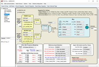
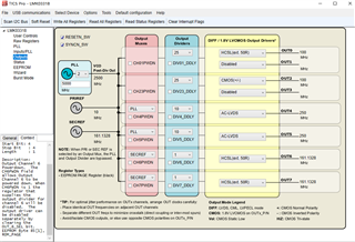
         2. the wizard in TICS PRO used for frequency point configuration.

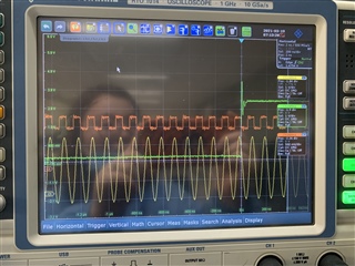
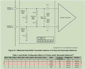
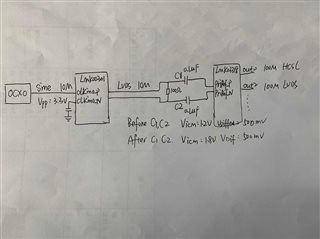
         3.the input clock is the LVDS level output by LMK00301, and there is an external AC capacitor.

         Not sure why the lock is unstable, do you have any debugging suggestions?


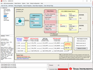
R0	0x0010
R1	0x010B
R2	0x0233
R3	0x0301
R4	0x0400
R5	0x0500
R6	0x0600
R7	0x0700
R8	0x0800
R9	0x0900
R10	0x0AA0
R11	0x0B00
R12	0x0CD9
R13	0x0D00
R14	0x0E1D
R15	0x0F00
R16	0x1000
R17	0x1100
R18	0x1200
R19	0x1300
R20	0x1455
R21	0x1555
R22	0x16FF
R23	0x1703
R24	0x1800
R25	0x195A
R26	0x1A00
R27	0x1B28
R28	0x1C08
R29	0x1D03
R30	0x1E00
R31	0x1F58
R32	0x2000
R33	0x2118
R34	0x2278
R35	0x2300
R36	0x2418
R37	0x2510
R38	0x2609
R39	0x2710
R40	0x2809
R41	0x29EC
R42	0x2A00
R43	0x2BEC
R44	0x2C00
R45	0x2D1A
R46	0x2E00
R47	0x2F00
R49	0x3100
R50	0x3256
R51	0x3303
R52	0x3400
R53	0x3500
R54	0x3600
R55	0x3700
R56	0x3806
R57	0x3908
R58	0x3A01
R59	0x3BF4
R60	0x3C00
R61	0x3D00
R62	0x3E00
R63	0x3F00
R64	0x4000
R65	0x4101
R66	0x420C
R67	0x4338
R68	0x4401
R69	0x4504
R70	0x4607
R71	0x471F
R72	0x4808
R73	0x4900
R74	0x4A64
R75	0x4B00
R76	0x4C00
R77	0x4D00
R78	0x4E00
R79	0x4F00
R80	0x5001
R81	0x510C
R82	0x5224
R83	0x5300
R84	0x5400
R85	0x5500
R86	0x5600
R87	0x5700
R88	0x5800
R89	0x59DE
R90	0x5A01
R91	0x5B18
R92	0x5C01
R93	0x5D4B
R94	0x5E01
R95	0x5F86
R96	0x6001
R97	0x61BE
R98	0x6201
R99	0x63FE
R100	0x6402
R101	0x6547
R102	0x6602
R103	0x679E
R104	0x6800
R105	0x6900
R106	0x6A05
R107	0x6B0F
R108	0x6C0F
R109	0x6D0F
R110	0x6E0F
R115	0x7308
R116	0x7419
R117	0x7500
R118	0x7607
R119	0x7701
R120	0x7800
R121	0x790F
R122	0x7A0F
R123	0x7B0F
R124	0x7C0F
R129	0x8108
R130	0x8219
R131	0x8300
R132	0x8403
R133	0x8501
R134	0x8600
R135	0x8700
R136	0x8800
R137	0x8910
R138	0x8A00
R139	0x8B00
R140	0x8C00
R141	0x8D00
R142	0x8E00
R143	0x8F00
R144	0x9000
R145	0x9100
R169	0xA940
R172	0xAC24
R173	0xAD00
R12     0x0C59
R12     0x0CD9

  • Hello Xin Li,

    Please advise what frequency was being input to device, as well as voltage level. After PLL became unstable was the output of the LMK00301 checked or the input to LMK00301?

    Using the attached register in TICSPRO shows me that the Fvco probably was not set correctly as Fvco of LMK03318 should be between 4.8 - 5.4 GHz.

  • hello Aaron:

                        Use the oscilloscope trigger mode, green is status 0, 1 is lock out and 0 is locked. Orange is the signal point tested before the AC coupling capacitor at the input of LMK03318. Green is the input of lmk00301, which is a 10MHz single-ended sine signal. When the lock was lost, no fluctuations in the clock were seen. We also tested 1.8v and 3.3v power supplies, and there was no jitter or other abnormalities when the lock was lost. Do you have any special suggestions? Looking forward to your reply, thank you!

  • hello Aaron,

                        Our design Fvco is 5GHz,,as follows ,Is there any problem with the register configuration? Please explain in details.

           I want to ask a question. According to the instructions in the manual, if it is external LVDS AC coupling, LMK03318 needs to enable           TERMINATION and BIASING internally. When I select "diffterm_pri" and "AC mode pri" at the same time. The register is configured as 0X1D05, the indicator light of the statues1 will indicate no input. When I only select "AC mode pri" and the register configuration is 0X1D01, I can measure that the common mode voltage is 1.8V, and the configuration takes effect. The indicator of the statues1 is normal, showing that PRIREF has input. I don’t understand that it’s not OK to select it at the same time.

    Statues0 and statues1 are connected to external lights as lock and input indication signals, both of which are active low and the lights are on.

    The clock structure and clock level are as followsThe clock structure and clock level are described in the following figure.   

    waiting for your reply, thank you!


  • Hello Xin Li,

    There are a couple of things we can check both are related to the PRI S-E Detect Mode, #1 should be tested first then #2:

    1. Please set PRI S-E Detect Mode located in the 'Inputs/PLL' tab to Vih/Vil Level detect

    2. Keeping PRI S-E Detect Mode to Vih/Vil change PRI Diff Detect Level to 300 mVpp Diff swing and 200 mVpp.

    The reason why this might be having an issue is because currently Loss of Signal is set to 'Slew Rate Detect' and this has seen an issue in the past.

  • Hello Aaron,

    I tried the suggestions you recommended, but the actual measurement is still unstable. I tried to change the "Ref Detector" to "Bypass", and the effect will still detect the loss of lock.

    We tested the input clock of LMK00301 and LMK03318, and used an oscilloscope to grasp the relationship between the loss of lock with the clock, and the relationship with the power supply, but no obvious problems were seen. Is there any problem with this chip? I don't understand.

    The current project is very urgent and affects the startup stability of the ARM chip. Please help Positioning problem,thank you!

  • Hello Xin Li,

    Please watch the LOS Status as well as the LOL Status to make sure we are maintaining a valid input - from the device's perspective.

    You can utilize the same oscilloscope setup you had previously just add another connection to detect LOS as you did with LOL or remove connection to buffer input.

    We also could check both the N and P side of the input, this might be helpful.

  • hi  Aaron,

    I changed the input to LMK00301 to square wave input. LMK00318 lock is much more stable than before, but some boards may lose lock several times. I would like to ask how to enable the input 100 ohm internal termination. When I enable “diffterm_pri”,wrote Register R0x1D as0x1D87, Statues "PRIREF LOS" will be detected without input. How can I enable internal termination?

  • Hello Xin Li,

    Please see section 10.4.2 of the Datasheet discussing the Universal Input Buffer available on PRI_REF and SEC_REF for a visual and Table 4. Input Buffer Configuration Matrix on Primary and/or Secondary Reference for refence.

    This table explains what registers to change (Register 50 [0x32] and 29 [0x1D]) based on what 'Mode' and 'External Coupling' you would like to utilize.

    From Register 0x1D setting of 0x87 you have chosen Internal Biasing / External AC Coupling and therefore External Coupling should be provided (Internal Biasing will be the same setting for all Modes). Has this case been met? Please share Register R13 settings.

  • Hello Aaron,

    I have seen section 10.4.2, the current design meets the LVDS external AC coupling, but after enabling the internal termination and bias, it detects "priref los" no clk input, I can confirm that the internal bias is enabled, but The internal termination does not seem to take effect.
    Also R13[0X0D00].

  • Hello Xin Li,

    Register 13 also looks like it is set correctly. If what you are claiming is correct, when you read back the device the settings of Register 50 (0x32) and 29 (0x1D) as well as the REF_SEL pin are all set to utilize PRIREF, correct?

    I think another read over of section 10.4.17 to 10.4.18.2 will be helpful. I will do this myself, sorry you are experiencing such a tedious issue.

  • hi  Aaron,

    Thank you for your reply. I tried to enable both "Diffterm_pri" and "Diffterm_sec" [0x1D0F]. The test found that the internal 100 ohm termination was enabled. It seems that only enabling one of the terminations (only "Diffterm_pri" or only "Diffterm_sec") the internal 100 ohm termination does not take effect. 

    The section 10.4.18.2  “The PLL’s loss of lock detection circuit is a digital circuit that detects any frequency error, even a single cycle slip. The PLL unlock is detected when a certain number of cycle slips have been exceeded”    When the above situation occurs, can the clock continue to be output? Instead of losing the lock and not outputting the clock, I tried to set R22 CH_0_MUTE to CH_7_MUTE to 0. Is this configuration OK?

  • Hello Xin Li,

    If you enable both 'Diffterm_pri' and 'Diffterm_sec' has this correctly enabled 100 ohm termination?

    If you would like to continue operation after Loss of Lock you can utilize R23 and set these bits to '0', if '1' is set the the STATUSx Output will be automatically disabled when the selected clock source is invalid. Please also note. you can utilized a slower STATUS1 or STATUS0 slew rate output through R49 which will help reduce coupling onto your high-speed outputs.

  • If you enable both 'Diffterm_pri' and 'Diffterm_sec' has this correctly enabled 100 ohm termination?

    yes

  • Hello Xin Li,

    Are you still seeing your issue or is this resolved?

  • When it is detected that the clock signal is out of lock, the system clock to ARM will not be output, (even though I set Channel MUTE to 0) ARM's startup and work will be affected in some cases. This happens occasionally in the current test, and I am still paying attention to this issue. Observation and pressure testing are underway.

  • Hello Xin Li,

    Please keep me updated with your observations I'll have to ask the internal team if they have seen this.