This thread has been locked.

If you have a related question, please click the "Ask a related question" button in the top right corner. The newly created question will be automatically linked to this question.

LMK04828: Technical problems of LMK04828

Part Number: LMK04828
Other Parts Discussed in Thread: LMK04832

Hi team,

I got question from customer.

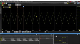
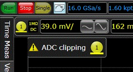
DCLK channel output of LVPECL 1600 format waveform, the output of the actual waveform swing is only more than 100 mV.

Please help with the analysis.

Thanks

Best regards,

  • Hi Zhonghui,

    At what frequency was the customer measuring?

    Do you have a TICS Pro profile (.tcs) or a hex register file from the customer showing how they configured the system?

    Has the customer confirmed that LVPECL termination is present on the output they are trying to measure?

    Regards,

    Derek Payne

  • Hi Payne

    The frequency is 122.88MHz,

  • Hi li li47,

    Are you using the default profile? If not, can you upload the TICS Pro profile you're using? You can drag and drop the .tcs file saved by TICS Pro into the E2E post window.

    Is this on the EVM? Which output are you measuring?

    I need more information, or it will be very challenging to determine what's happening.

    Regards,

    Derek Payne

  • HI Payne 

    The frequency is 122.88MHz,and the register file is as following.

    @000

    06000031 // SPI时钟分频50
    079800ff // SPI写操作,SPI数据位数24bit,设备选择
    08000090 // 复位
    08000090 //
    08000090 //
    08000000 // 正常工作
    08000200 // 不powerdown
    080100ff // clk0分频比24 输出频率122.88M
    08010155 // clk0延迟周期高和低的周期都是5
    08010300 // 模拟延迟为500ps+0ps
    08010420 // 设定clk0的SDCLK为sysref时钟输出,clk1 输出频率 3.072M ZU9 jesd204B clk
    08010500 // SDClk模拟延迟关闭,模拟延迟为0
    080106F0 // 数字时延,无故障半步功能,和时钟输出PD关闭,sysref正常操作,打开输出
    08010715 // 时钟输出电平DCLK out LVPECL 1600mV, sDCLK 输出 LVDS
    08010801 // clk2的分频比为1 输出频率2949.12M
    08010955 // clk2延迟周期高和低的周期都是5
    08010B02 // 模拟延迟为500ps+0ps
    08010C20 // SDclk1为sysref输出,延迟周期为0 clk3 输出频率 3.072M
    08010D10 // SDCLK1sysref模拟延迟打开,模拟延迟为0
    08010EF9 // 关闭输出 数字时延,无故障半步功能,和时钟输出PD关闭,sysref正常操作,
    08010F15 // 时钟输出电平LVPECL 1600mV ,SDC输出电平Lvds
    08011018 // clk4分频比24 输出频率122.88M ADRV9009 jesd204B clk
    08011155 // clk4延迟周期高和低的周期都是5
    08011300 // 模拟延迟为500ps+0ps
    08011420 // SDclk5为sysref输出,延迟周期为0 clk5 输出频率为3.072M
    08011500 // SDclk5模拟延迟关闭,模拟延迟为0
    080116F0 // 数字时延,无故障半步功能,和时钟输出PD关闭,sysref正常操作,打开输出
    08011715 // 时钟输出电平LVPECL1600mv,SDC输出LVDS
    08011818 // clk6分频比24输出频率122.88M
    08011955 //
    08011B00 //
    08011C20 // 设定clk6的SDCLK为设备时钟输出,输出时钟频率为245.76M
    08011D00 //
    08011EF0 // clk 正常输出,SDC 正常输出,
    08011F15 // 时钟输出电平LVDS,sDC输出LVDS
    08012018 // clk8 分频比24 输出频率122.88M
    08012155 //
    08012300 //
    08012420 // sysref输出 clk9 输出频率为3.072M
    08012500 //
    080126F9 // 关闭输出
    08012755 // 时钟输出电平LVPECL 1600mV ,SDC输出LVPECL 1600mV
    08012818 // clk10分频比24 输出频率122.88M
    08012955 //
    08012B00 //
    08012C00 // clk输出 clk11 输出频率122.88M
    08012D00 //
    08012EF9 // 关闭输出
    08012F55 // 时钟输出电平LVPECL 1600mV ,SDC输出LVPECL 1600mV
    08013018 // clk12分频比24 输出频率122.88M ZU9 jesd204B clk
    08013155 //
    08013300 //
    08013420 // sysref输出 输出频率为3.072M
    08013500 //
    080136F0 // 打开输出
    08013715 // 时钟输出电平LVPECL 1600mV ,SDC输出LVDS
    08013831 // OSCout的功能,时钟路径VCO1,oscout模式feedbackmux,oscout电平LVDS
    08013903 // sysref输出,源头,sysref源:sysref_mux,sysref_mux源:sysref pluse
    08013A00 // sysref分频比960 sysclk输出频率为3.072M
    08013B18 // sysref分频比960
    08013C00 // sysref数字延迟0
    08013D00 // sysref数字延迟0
    08013E03 // sysref是 pluse模式下的脉冲计数器值 ,计数值8
    08013F05 // PLL2 N divider : PLL prescaler,PLL1 N delay :oscin,Fbmux :sysref divider,Fbmux 使能
    08014000 // 全都不power down,
    08014100 // 不允许输出出现动态数字时延
    08014200 // 设置动态数字延迟的调整补偿,不调整
    0801431e // sync操作,sync mode 02, PLL1和PLL2锁定指示拉高的时候sync,sync管脚拉高的时候sync,
    080144FF // sysref不被sync掉
    0801457F // 固定值
    08014619 // clkin1和clkin0使能进入automode,clk0输入类型单端,clk1差分
    0801471A // PLL1固定输入为clkin1,clkin1的buffer 放在PLL1后面,clkin0的buffer也在PLL1后边
    08014813 // clkin_sel0功能: clkin0 selected,类型输出
    08014953 // SDIO功能,开漏输出,clkin1_sel1功能:clkin1selectd,输出管脚
    08014A02 // 复位功能,高电平复位,内置下拉电阻
    08014B76 // holdover功能,timeout时间2.1M,LOS功能打开,监测PLL1电荷泵电压,强制holdover关闭,手动dac模式自动进入,
    08014C00 // 手动DAC的值为0x200
    08014D00 // holderover模式下的不能低于的最高的值0
    08014EBF // dacmulti 16384,dac trip high 3.3
    08014F7F // dac_clk_counter 127
    08015049 // 时钟切换功能相关,默认
    08015102 // 从holdover切换回正常模式PLL1需要的有效时钟数量 ,默认
    08015200 // 从holdover切换回正常模式PLL1需要的有效时钟数量 ,默认
    08015300 // clkin0的分频器,125
    0801547D // clkin0的分频器,125
    08015501 // clkin1的分频器,400
    08015690 // clkin1的分频器,400
    08015700 // clkin2的分频器,150,默认值
    08015896 // clkin2的分频器,150,默认值
    08015906 // PLL1 N分频器值,1600
    08015A40 // PLL1 N分频器值,1600
    08015BDF // PLL1的鉴相器,数字鉴相器的窗口值,43ns,锁相环CP端增益1550uA,
    08015C20 // PLL1 DLD的鉴相器 窗口值 8192,默认
    08015D00 // PLL1 DLD的鉴相器 窗口值 8192,默认
    08015E00 // PLL1 N和R的延迟,默认
    08015F0B // PLL1 LD管脚功能:PLL1 DLD,输出模式,
    08016000 // PLL2 R分频器值2
    08016102 // PLL2 R分频器值2
    08016244 // PLL2 功能,PLL2 N分频器值2,osc频率值范围127-255M,osc放大关闭,双倍的频率也关闭,
    08016300 // PLL2_Ncal值,12默认
    08016400 // PLL2_Ncal值,12
    0801650C // PLL2_Ncal值,12
    080171AA // 固定值
    08017202 // 固定值
    08017C15 // 选器件
    08017D33 // 选器件
    08016600 // PLL2n分频器值,24 VCO输出频率2949.12M
    08016700 // PLL2n分频器值,24
    08016818 // PLL2n分频器值,24
    08016959 // PLL2鉴相器功能,3.7ns,cp增益3200uA,
    08016A20 // PLL2 DLD计数器值,8192
    08016B00 // PLL2 DLD计数器值,8192
    08016C00 // PLL2内置环路滤波器参数,R3,200欧姆,R4,200欧姆
    08016D00 // PLL2内置环路滤波器参数,c3,10pF,C4,10pF
    08016E13 // PLL2_LD功能: PLL1dld,输出
    08017300 // PLL2 正常操作,
    081FFD00 //
    081FFE00 //
    081FFF53 //
    09000001 // sync LMK04828
    00000000 //
    09000000 // 取消sync LMK04828
    00000000 // SPI读操作,SPI数据位数24bit,设备选择
    075800ff //
    08800000 //
    08800200 //
    08810000 //
    08810100 //
    08810300 //
    08810400 //
    08810500 //
    08810600 //
    08810700 //
    08810800 //
    08810900 //
    08810B00 //
    08810C00 //
    08810D00 //
    08810E00 //
    08810F00 //
    08811000 //
    08811100 //
    08811300 //
    08811400 //
    08811500 //
    08811600 //
    08811700 //
    08811800 //
    08811900 //
    08811B00 //
    08811C00 //
    08811D00 //
    08811E00 //
    08811F00 //
    08812000 //
    08812100 //
    08812300 //
    08812400 //
    08812500 //
    08812600 //
    08812700 //
    08812800 //
    08812900 //
    08812B00 //
    08812C00 //
    08812D00 //
    08812E00 //
    08812F00 //
    08813000 //
    08813100 //
    08813300 //
    08813400 //
    08813500 //
    08813600 //
    08813700 //
    08813800 //
    08813900 //
    08813A00 //
    08813B00 //
    08813C00 //
    08813D00 //
    08813E00 //
    08813F00 //
    08814000 //
    08814100 //
    08814200 //
    08814300 //
    08814400 //
    08814500 //
    08814600 //
    08814700 //
    08814800 //
    08814900 //
    08814A00 //
    08814B00 //
    08814C00 //
    08814D00 //
    08814E00 //
    08814F00 //
    08815000 //
    08815100 //
    08815200 //
    08815300 //
    08815400 //
    08815500 //
    08815600 //
    08815700 //
    08815800 //
    08815900 //
    08815A00 //
    08815B00 //
    08815C00 //
    08815D00 //
    08815E00 //
    08815F00 //
    08816000 //
    08816100 //
    08816200 //
    08816300 //
    08816400 //
    08816500 //
    08816600 //
    08816700 //
    08816800 //
    08816900 //
    08816A00 //
    08816B00 //
    08816C00 //
    08816D00 //
    08816E00 //
    08817300 //
    08817C00 //
    08817D00 //
    089FFD00 //
    089FFE00 //
    089FFF00 //
    08817400 //
    08818200 //
    08818300 //
    08818400 //
    08818500 //
    08818800 //
    08800300 //
    08800400 //
    08800500 //
    08800600 //
    08800c00 //
    08800d00 //
    08817100 //
    08817200 //
    00000000 //
    079800ff //SPI写操作,SPI数据位数24bit,设备选择
    0801447F //阻止时钟输出被sync信号或者sysref信号输出的时候给同步了
    0801447C //阻止时钟输出被sync信号或者sysref信号输出的时候给同步了,除了clk0和clk2
    08014331 //sync极性反转,使能sync功能,sync模式,事件从sync管脚进行同步
    080144F9 //防止SYSREF信号被SYNC信号给同步了,clk也是,除了clk0和clk2,(Z7和V7的DAC的时钟)
    080144FB //防止SYSREF信号被SYNC信号给同步了,clk也是,除了clk2(V7的DAC时钟)
    080144FF //防止SYSREF信号被SYNC信号给同步了,clk也是,
    080106F0 //dac开sysref
    00000000 //
    080106F1 //dac关sysref
    00000000 //
    079800FF //SPI写操作,SPI数据位数24bit,设备选择
    08013900 //sysref的源是SYNC信号
    08014311 //sync使能,sync模式,从sync管脚同步,
    08014000 //sysref正常操作
    08014407 //允许sysref被sync同步,允许V7的ADC时钟和DAC时钟和DAC时钟被sync同步
    08014311 //sync使能,sync模式,从sync管脚同步,
    08014331 //sync极性反转,使能sync功能,sync模式,事件从sync管脚进行同步
    08014311 //sync使能,sync模式,从sync管脚同步,
    080144FF //防止SYSREF信号被SYNC信号给同步了,clk也是,
    08013903 //sysref的源是连续的SYSref信号
    00000000 //
    08010F55 //ADCCLK
    08010EF0 //开sysref
    00000000 //
    08010F55 //
    08010EF1 //关sysref
    08010801 //adc时钟分频
    00000000 //

    I do not have the EVM,I designed the circuit of lmk04828 ,the out put imeasured are DCLK0,DCLK12,dclk4 and dclk6.

    Thanks for anwsering me .

  • Hi Ii Ii,

    We are still not sure on the LVPECL termination for DCLK0,DCLK12,dclk4 and dclk6 ports in your design. If you are following the LMK04828EVM design, where only DCLK0 and DCLK2 are terminated with 240ohm resistors for LVPECL output format. Please confirm for DCLK12,dclk4 and dclk6 also you have provided same 240ohm termination? would be helpful, if you can share the LMK04828 section schematic for better understanding?

    080100ff // clk0分频比24 输出频率122.88M

    For 122.88MHz at clk0 output, 0x100 register values should be 0x18 (divider - 24) but your shows FF, which is not correct setting and may provide some abrupt output. 

    Are you getting the LVPECL amplitude issue at all ports DCLK0,DCLK12,dclk4 and dclk6? same frequency, same amplitude?

    Regards,

    Ajeet Pal

  • Hi Pal

    The 0x100register value is 0x18, the former value of FFis the wrong one I had write in the register. I had corrected the value to 0x18. All the Dclk channels I used all have the amplitude issue. I have the termated resistors in my schematic and the board .And I had changed the value of the termated resisters from 90ohm to 240ohm, but it did not matter to the amplitude issue.

    lmk04828.pdf

  • hi Pal

    The following image is the wave I had tested , just to be used to analyze fou you.

    best regards

    thanks

  • li li,

    I'm not seeing anything wrong with the register settings after correcting the divider value.

    What is the schematic of the receiver section? is the load 2x 50Ω single-ended or 100Ω differential? DC- or AC-coupled?

    Regards,

    Derek Payne

  • Hi Payne

    The receiver of the 122.88Mhz is FPGA and the refclk of ADRV9009,in my schematic there is no load of 2X50ohm single-ended or 100ohm differential,but when I tested the board, I soldered a 100ohm differential across the AC coupled capacitors, but it did not matter to the amplitude issue. AC-coupled to the Dclk channel. The schematic of receiver is like this as following .

    Best regards to you.

  • Hi Payne 

    When I tested my board, I also changed the AC-coupled capacitors from 0.1uF to 0.01uF, but it also did not matter.

  • li li,

    I'm not sure what's going on. The register settings appear correct, the channels are not being synchronized, the divide value is even so no duty cycle correction should be required, the emitter biasing appears correct, and otherwise there do not appear to be any issues with the schematic or the registers. I only have two remaining thoughts as to what could be going on:

    First, I see from your previous plot that the impedance at the probe is 1MΩ DC:

    Is it possible that the shunt capacitance in parallel with the probe resistance is causing the output amplitude to degrade? Trying to directly drive a large capacitive load with an AC signal would definitely bring the amplitude down. Is there some way to measure just the output into AC-coupled 50Ω?

    My other thought: Can you replicate this issue on multiple boards? Maybe the output buffer was damaged with 90Ω emitter resistor biasing on LVPECL20. I don't think this is likely, because the LMK04832 has an internal current limit that should prevent damage if the output is shorted or overloaded... alternately, maybe the output is still overloaded somehow, and you are observing a small feed-through signal from an otherwise-shorted output.

    Regards,

    Derek Payne