Dear,
For a project in development, we work with the ZCU102 Evaluation Kit (including Zynq UltraScale+ ZU9EG) for a demonstrator.
And to drive RF switch from 50 MHz (with Duty cycle at 50% max) to ~ 3.3MHz (with duty cycle at 3%), we use LVDS interface of FPGA.
I was looking for a buffer LVDS, with one input and several outputs, and I find LMK00306 from TI.
Several LMK00306 are used (qty = 5), to drive 15 RF switch at the same time (with a margin).
Each LMK 00306 has a synchronized LVDS signal generated by the FPGA.
For us, timings Trise and Tfall are very important. With LMK00306, 300ps for Tr and Tf, it's acceptable.
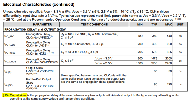
I am looking to assess the min / max delay between the slowest and the fastest of the control signals, to know the margin.
It has specification of Duty cycle (page 9 of datasheet), specififed between 45% to 55% for 50% input clock duty cycle. And Output Skew Timing on page 13.
How understand these informations, on pages 9 and 13 of LMK00306 datasheet, about "Output Clock duty cycle" and "Duty Cycle skew" ?
For a signal on input of LMK00306, What signal do I find at the output ?
With what delay ?
Thanks.
Best Regards.
Arnaud CHOPIN