Because of the Thanksgiving holiday in the U.S., TI E2E™ design support forum responses may be delayed from November 25 through December 2. Thank you for your patience.

This thread has been locked.

If you have a related question, please click the "Ask a related question" button in the top right corner. The newly created question will be automatically linked to this question.

CDC3RL02: clarification on the value of sine wave input

Part Number: CDC3RL02

Hello Guys,

Good day.

In the datasheet it writes several times that the lowest acceptable sine-wave input is 0.3 Volts, but In the typical characteristics graph it shows the typical sine-wave input swinging from 0V to 1.8V
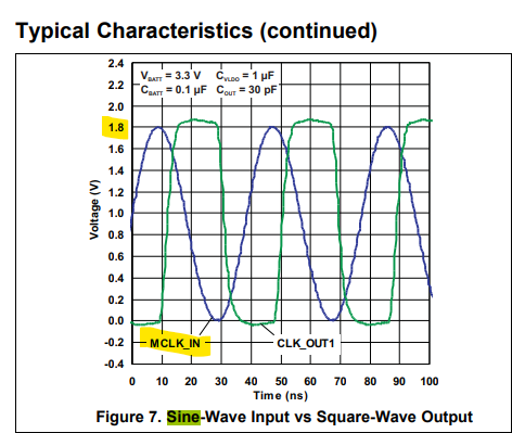

In the electrical specifications it shows the lowest as being .3V but is that P-P? In the actual typical characteristics on page 8 it shows a sine wave swinging from 0 to 1.8V being used as the MCLK_IN.

Thanks for the confirmation.

Art

  • Hi Art,

    The input amplitude is defined as P-P in this datasheet. This means that the buffer accepts a minimum amplitude of 0.3V and maximum of 1.8V.

    In the Typical Characteristics section, the figure means to show the characteristics of a 1.8V MCLK_IN input (0 to 1.8V). If a 0.3V MCLK_IN input is to be used, then a 0 to 0.3V sinewave would be shown.

    Regards,

    Jennifer