Dear Representative,
We use CDCM6208V1 as main clock generator in our device, But also we want to use CDCM6208V2 as alternative.
Our configuration for CDCM6208V1 is(check by EVM tool):
Y0: LVDS 125 MHz
Y1: LVDS 125 MHz
Y2: LVDS 100 MHz
Y3: LVDS 100 MHz
Y4: HCSL 100 MHz
Y5: HCSL 100 MHz
Y6: HCSL 100 MHz
Y7_1: LVCMOS 25MHz
Y7_2: LVCMOS 25MHz
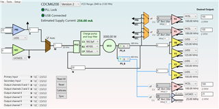
But same EVM tool for CDCM6208V2 show next configuration:
Y0: LVDS 100 MHz
Y1: LVDS 100 MHz
Y2: LVDS 125 MHz
Y3: LVDS 125 MHz
Y4: HCSL 100 MHz
Y5: HCSL 100 MHz
Y6: HCSL 100 MHz
Y7_1: LVCMOS 25 MHz
Y7_2: LVCMOS 25 MHz
As you can see there is difference in configuration between Y0..Y4 port for CDCM6208V1 and V2. So, for compatibility between CDCM6208V1 and V2 we need extra 0R resistors jumpers on PCB.
Can you please check, is it really impossible to configure CDCM6208V1 and CDCM6208V2 identically without adding extra 0R jumpers for compatibility during PCBA?
Thank you!