This thread has been locked.

If you have a related question, please click the "Ask a related question" button in the top right corner. The newly created question will be automatically linked to this question.

LMK00338: PCB layout for unused output pins

Part Number: LMK00338

Hi team,

As written on the datasheet 8.3.3 Clock Outputs, any unused output pin should be left floating with a minimum copper length (see note below) to minimize capacitance and potential coupling and reduce power consumption.

And This way during reflow, the solder has the same copper area as connected pins. This allows for good, uniform fillet solder joints helping to keep the IC level during reflow.

Sorry, I couldn't understand what this mean.  The below undestanding is correct?

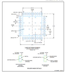
Unused output pins should be left open, but it recommneds that unused ouput pins are also connected as other pins to make the IC connected well to the board. And the picture as below is good example as the soleder mask for unused pins. The picture comes from P.33 of the datasheet.

Could you also expain " the IC level " of  8.3.3 Clock Outputs?

Regards,

Noriyuki Takahashi

  • Hi Takahashi-san,

    Unused output pins should still have PCB pads in the footprint (as described in the solder mask image) to ensure the mechanical stresses on the package are equally distributed, but the pads do not need to be electrically connected to any other copper on the PCB.

    I think 8.3.3 is referring to visible pad area during reflow. Pad size may be similar, but if the area of the metal exposed by the soldermask is different on different pads, the surface tension created by the wet solder on the different sides of the IC may be different. Differing surface tension on different sides of the IC during reflow can prevent some corners or sides of the package from aligning flat on the PCB, so the device may not sit level (synonym for flat) on the PCB. In practice, I think this means that the exposed metal should be extended slightly beyond the pad as if there was a trace connecting to it, so the total surface area and geometry of each exposed metal pad is kept similar when possible.

    I think we may have had a customer in the past who used only outputs on one side of the IC, and the IC did not form uniform fillet joints on both sides of the device, so the chip tilted during reflow. By running the unused output traces just past the edge of the soldermask, the surface tension of the fillet joints on the unused side was equalized, and the IC would sit flat during reflow.

    Regards,

    Derek Payne