Other Parts Discussed in Thread: TIDA-01021, LMX2594, , LMK00804B, LMK61E2
Hi,
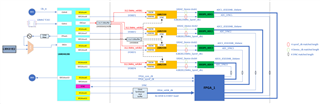
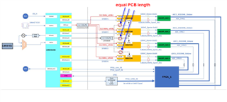
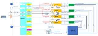
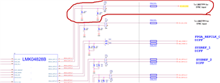
I would like to use LMK04828B+LMK2594 to provide device clock(10GHz) and sysref(4.8828125Mhz) clock to 4pcs ADC at the same time, and realize multichannel clock solution with phase alignment.
It is important that 4pc ADC sample synchronously, so clock scheme should be selected to minimize the sampling skew. I plan to use JESD204B subclass1 to realize multi-chip synchronization,
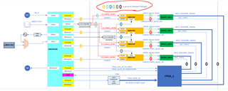
As below figure shown, which clock scheme would be better to realize the lower phase noise DEVCLK generation and multichannel clock solution with phase alignment? Option1 or Option2?
Thanks in advance!
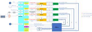
Option1:
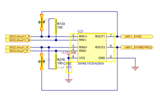
Option2: refer to design of TIDA-01021 partially