This thread has been locked.

If you have a related question, please click the "Ask a related question" button in the top right corner. The newly created question will be automatically linked to this question.

LMK04832: Unsure of Validity of Clock Outputs

Part Number: LMK04832
Other Parts Discussed in Thread: LMX2594,

Hello,

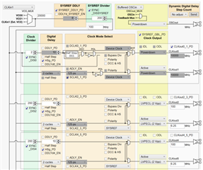
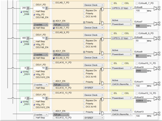
I am using a commercial board that has an LMX04832 feeding three LMX2594 as well as numerous FPGA pins directly. In using TICS PRO to create the register programming file for the LMK, it doesn't complain about anything, even when I enter an output frequency of 800GHz, so I wanted to verify with you all that my clock setup is valid. I am using a 100MHz external reference on CLKin1. I have attached the register text file as well as screenshots of my current clock output configuration in the TICS app in case the registers load incorrectly.

Thanks

  • lmk04832_100MHzRef_100MHzLMX_6MHz25SYSREF_50MHzPLCLK.txt
    R0 (INIT)	0x000090
    R0	0x000010
    R2	0x000200
    R3	0x000306
    R4	0x0004D1
    R5	0x000563
    R6	0x000650
    R12	0x000C51
    R13	0x000D04
    R256	0x010002
    R257	0x01010A
    R258	0x010280
    R259	0x010340
    R260	0x010410
    R261	0x010500
    R262	0x010601
    R263	0x010700
    R264	0x0108C8
    R265	0x01090A
    R266	0x010A00
    R267	0x010B40
    R268	0x010C20
    R269	0x010D00
    R270	0x010E01
    R271	0x010F55
    R272	0x0110C8
    R273	0x01110A
    R274	0x011200
    R275	0x011340
    R276	0x011420
    R277	0x011500
    R278	0x011601
    R279	0x011755
    R280	0x0118C8
    R281	0x01190A
    R282	0x011A00
    R283	0x011B40
    R284	0x011C10
    R285	0x011D00
    R286	0x011E01
    R287	0x011F05
    R288	0x012090
    R289	0x01210A
    R290	0x012201
    R291	0x012340
    R292	0x012410
    R293	0x012500
    R294	0x012601
    R295	0x012705
    R296	0x012808
    R297	0x01290A
    R298	0x012A00
    R299	0x012B40
    R300	0x012C20
    R301	0x012D00
    R302	0x012E01
    R303	0x012FF0
    R304	0x013002
    R305	0x01310A
    R306	0x013200
    R307	0x013340
    R308	0x013420
    R309	0x013500
    R310	0x013601
    R311	0x0137C0
    R312	0x013840
    R313	0x013903
    R314	0x013A00
    R315	0x013BC8
    R316	0x013C00
    R317	0x013D08
    R318	0x013E03
    R319	0x013F80
    R320	0x01408B
    R321	0x014100
    R322	0x014200
    R323	0x014311
    R324	0x0144FF
    R325	0x014500
    R326	0x014610
    R327	0x014712
    R328	0x014802
    R329	0x014902
    R330	0x014A03
    R331	0x014B06
    R332	0x014C00
    R333	0x014D00
    R334	0x014EC0
    R335	0x014F7F
    R336	0x015001
    R337	0x015102
    R338	0x015200
    R339	0x015300
    R340	0x015478
    R341	0x015500
    R342	0x015678
    R343	0x015700
    R344	0x015896
    R345	0x015900
    R346	0x015A78
    R347	0x015BD4
    R348	0x015C20
    R349	0x015D00
    R350	0x015E1E
    R351	0x015F3B
    R352	0x016000
    R353	0x016101
    R354	0x01624C
    R355	0x016300
    R356	0x016400
    R357	0x01650C
    R361	0x016958
    R362	0x016A20
    R363	0x016B00
    R364	0x016C00
    R365	0x016D00
    R366	0x016E13
    R371	0x017310
    R375	0x017700
    R386	0x018200
    R387	0x018300
    R358	0x016600
    R359	0x016700
    R360	0x016864
    R1365	0x055500
    

  • Cameron,

    It's not clear to me what you're trying to do. Can you please provide a little more detail, such as the intended input and output frequencies, the clock outputs that should be active, whether you're trying to use distribution mode or you need the PLL/SYSREF features, etc. Per the datasheet it shouldn't be possible to provide a 20GHz clock on CLKin1 and still have the device work, so there's something wrong with this configuration.

    Regards,

    Derek Payne

  • Derek,

    Apologies for a confusing post. To clarify the remark about attempting to enter 800GHz: I am accustomed to TICS Pro highlighting something in red when you enter a value that is not possible or will not work with the configuration (this happens with TICS Pro and the LMX2594), however no red highlighting occurs for the LMK04832. Thus I was wanting to know from you all if my configuration is valid, since TICS wasn't throwing any errors, even for a bogus number of 800GHz.

    To clarify my desired configuration, it's as follows:

    100MHz reference on CLKin1
    CLKout0 and CLKout1 disabled
    CLKout2, CLKout4, and CLKout6 at 100MHz LVPECL2Vpp (Device Clock I believe, since they go to three LMX2594 chips)

    CLKout3 and CLKout5 at 6.25MHz LVPECL2Vpp (continuous running SYSREF I believe, since they serve as SYSREF clocks for an FPGA ADC/DAC)

    CLKout8 at 50MHz LVPECL2Vpp (Device Clock I believe, since it is just used as a normal clock on the FPGA)

    CLKout11 and CLKout13 at 100MHz CMOS Normal/Normal (SYSREF I believe)

    Some other notes: connected to CLKin0 is an on-board 12.288MHz TCXO and connected to OSCin_P/N is an on-board 122.88MHz VCXO. I don't want to use CLKin0 though, only CLKin1 since that's a 100MHz external reference clock.

    To be honest, I have gotten myself quite confused, so I'm not sure if this should be running in Distribution mode or PLL1 or PPL2, and what other settings are necessary, like on the SYNC/SYSREF, PLL1 and 2, and CLKinX Control pages.

    Hopefully this has been more clear, so any help in configuring this chip would be greatly appreciated, thanks!

  • Cameron,

    A quick primer on the differences between dual-loop (PLL1 + PLL2 cascaded), single-loop (PLL2-only), and distribution mode:

    • Dual-loop utilizes both PLLs, with PLL1 at a low bandwidth and PLL2 at a higher bandwidth. PLL1 acts as a "jitter cleaner" in the sense that it has a low bandwidth and a relatively clean VCXO that rolls off reference noise very effectively even for high-noise reference inputs. Since PLL1 is low bandwidth, there is rarely a large penalty for reducing the phase detector frequency, so PLL1 can also be used to translate frequencies to domains with very low GCD (such as 100MHz and 122.88MHz, which only share a GCD of 160kHz). PLL2 acts as a frequency multiplier with a high bandwidth, since the reference to PLL2 is a clean VCXO signal and there are phase noise advantages to running the phase detector frequency and loop bandwidth much higher than PLL1. PLL2 is used to generate an LCM frequency, or a multiple of the LCM frequency, so that all other clocks can be divided down.
    • Single-loop utilizes PLL2 exclusively. As long as the reference input is already clean on arrival, PLL2 can behave exactly like it does in the dual-loop configuration. 
    • Distribution mode bypasses all the PLLs and directly passes the output to the clock distribution path, instead of using a higher-frequency VCO output. This is conceptually straightforward, but there are some drawbacks (the resolution of digital delay is based on the period of the clock distribution frequency, so step size will be smaller in a PLL mode than in distribution mode unless the distribution input is very high frequency; SYSREF divider minimum divide value is 8, which imposes restrictions on the usable reference input frequency).

    We can try both the PLL2-only and distribution mode configurations (since you don't have a suitable VCXO frequency for the 100MHz, 50MHz, and 6.25MHz clocks to be derived from PLL2 with a high phase detector rate, running in dual-loop mode is not a great idea).

    For PLL2-only mode, I click Set Single Loop in the Set Modes page of TICS Pro. I configure CLKin1 as the input reference (CLKin1_DEMUX set to PLL1, CLKin_SEL_MANUAL set to CLKin1 Manual, PLL2_RCLK_MUX set to PLL1 CLKinX) and power down OSCin (OSCin_PD = 1). Since I happen to know that VCO0 has slightly better phase noise than VCO1, and all your frequencies can be derived from PLL2 VCO of 2500MHz, I can set VCO_MUX to VCO0 and set the N-divider and N-prescaler to 5 and 5 respectively. I also set the N cal divider alongside the N-divider, for reasons that are explained in greater detail in the datasheet (look for VCO calibration) but which are unimportant right now. I then configure the output dividers and SYSREF as needed to produce the configuration below. Note that it doesn't seem possible to use a 6.25MHz SYSREF from the SYSREF divider alongside a 100MHz CMOS SYSREF, since the whole point of SYSREF in JESD204B is that it's the GCD frequency (or an integer divisor thereof) of all clocks in the data converter system - I selected this to be 100MHz continuous from device clock instead of SYSREF. Also note that when using an odd divider value, the duty cycle correction bit (DCLKx_y_DCC) must be set to 1 to achieve proper 50% duty cycle.

    PLL2-only.tcs

    For distribution mode, I click Set Distribution in the Set Modes page of TICS Pro. This powers down all the PLL components for me. I set the SYSREF divider to 16 instead of 400 since my clock distribution is now at 100MHz. All 100MHz clocks are configured with DCC + HS set, since this is required for divide-by-1.

    distribution.tcs

    For now, synchronization and getting phase alignment between all the outputs is going to be left as an exercise for the reader (see section 8.3.4.1 in the datasheet). There is a step-by-step example of getting phase alignment offered in the datasheet.

    ---

    Regarding highlighting, the state of the LMK04832 GUI is pretty abysmal. I've been looking for a good justification to take the time to polish it for a while, and now seems as good a time as any... an improved version should be available either later this week or sometime next week.

    Regards,

    Derek Payne

  • Awesome, thank you so much for the in depth response/education as well as the attached TICS files! I really appreciate the help, I was feeling rather lost in what settings to use. Haha sounds good, I'll keep an eye out for that.