This thread has been locked.

If you have a related question, please click the "Ask a related question" button in the top right corner. The newly created question will be automatically linked to this question.

LMK00338:

Part Number: LMK00338

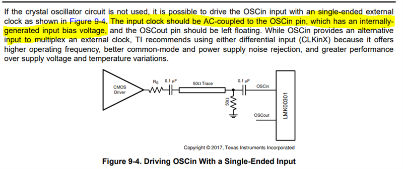
1- Would I be damaging OSCin inside buffer by applying a CMOS OSCILLATOR output directly to OSCin pin? The OSC's 3.3V CMOS output is divided by 2 via 2 x 49.9 ohms and fed to pin 13 (OSCin). no AC coupling cap is implemented.

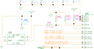
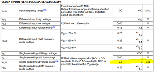
2- Am I over driving the CLK_IN_X_P/N by feeding these inputs with a greater than 1.3V swing clock signal? I am not getting anything at the outputs, so I thought may be I should bring the input amplitude down.

Thanks,

Bahram

  • Hi Bahram, 

    1. AC coupling is required for OSCin pin since there is an internal bias voltage. This would change the correct biasing condition in your case because of CMOS output. Please refer to this note in datasheet. 

    2. Please use the differential swing below 1.3V as specified in datasheet for CLK_IN_X_P/N and make sure CLKoutA_EN and CLKin_SEL0/1 are properly configured for desired clock input.

    Best,

    Asim

  • Asim,

    Thanks for your reply. AC coupling of OSC's CMOS output solved my issue. What is the max limiting amplitude on OSCin to prevent over drive? Any voltage divider will soften the slew rate.

    Bahram

  • Hello, 

    E2E is currently undergoing maintenance and will be unavailable until Monday, October 2nd. Responses will be delayed but we will get back to you as soon as possible. 

  • Hi Bahram,

    Since the OSCin design is similar to CLK_IN_X_P/N input stage. Please use the same amplitude limits (2V max) listed for single ended input in the datasheet. I have referenced that below.