Other Parts Discussed in Thread: LMK00304, LMK1D1204P,
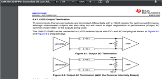
In the past, there has been a discussion about where the termination resistor should be placed in relation to LVDS AC coupling.
The link below is a discussion of the location of the termination resistor.
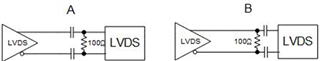
Assuming that there is a weak bias inside the LVDS receiver, there is no difference if there is a clock at the input of both A/B structures.
If the clock is not input to the input pin, the structure of A has a possibility of chattering and
The structure of B explains that it has the advantage of maintaining a certain state without chattering.
However, TI often responds by recommending the B structure.
However, in reality, application examples are provided in the datasheet by mixing various A/B structures.
This makes it very confusing in practical applications.
The links and datasheets below are some examples to confuse you.
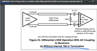
e2e.ti.com/.../lmk00308-lvds-outputs-with-ac-coupling-to-receiver-with-internal-100-ohm-termination
LMK00304
LMK1D1204P
So, I ask again about LVDS AC coupling as below, and hope it gets sorted out.
If there is a constant clock on the receiver input, my personal opinion is that the A structure is good.
The reason is the duty-cycle change.
TI says that there is no duty-cycle change according to the A/B structure, but this answer applies when the clock's rising/falling time is very very small or the frequency is low( f<100MHz ).
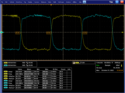
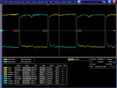
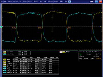
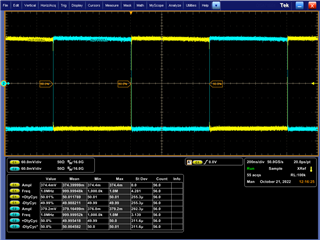
Actually, considering the rising/falling time of the input signal, it is thought that the duty-cycle change occurs as the frequency increases.
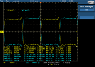
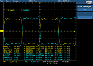
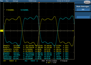
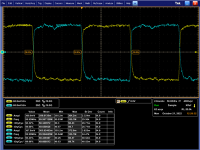
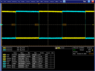
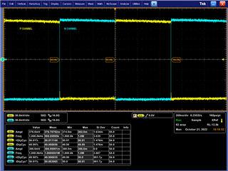
That is, below 100 MHz (approx. duty cycle = 50%), the duty cycle change is hard to see, but at 200 MHz, the duty cycle change is visible.
The reason for this is the different offset settings of P/N to prevent chattering.
Therefore, if the A structure is used, the other offset of P/N applied to prevent chattering is ignored and the P/N offset of the signal is equal to about 1.2V, so that the duty-cycle change does not occur even for a 200MHz signal.
In the case of LVDS AC coupling, if the clock continues to exist at the receiver input, is there any structure in the above A/B structure that is particularly problematic?
Is structure B still good?
Also I hope to provide a PSpice model for the clock buffer.
best regards
Lee HG