This thread has been locked.

If you have a related question, please click the "Ask a related question" button in the top right corner. The newly created question will be automatically linked to this question.

LMK00338: Outputs of the LMK00338 PCIe clock buffer are "dying" with time.

Part Number: LMK00338
Other Parts Discussed in Thread: LMK00334

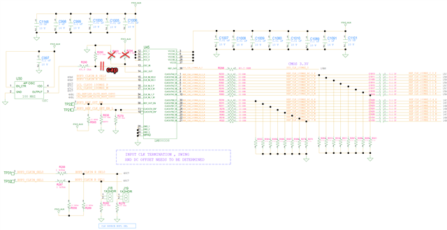
I have problem with LMK00338 8-Output PCIe clock buffer. The outputs are "dying" with time for unknown reason.

For instance, the swing of the positive or negative leg of some outputs could become about a half of a full swing. Some outputs are just not responsive (dead).

Also, after some time (10 minutes) all output could become unconscious (happen sometimes). They will be recovered after a short power down break.

  • Hi Alex,

    Thanks for posting your concern. This is not the expected operation of the device. Could you share some additional information listed below?

    • Can you tell if you are using TI EVM or part in your system? if its later, please share your schematic.
    • Could you also share that device was not stressed during the its operation beyond the recommended datasheet conditions?
    • Please share your measurement method as well and possible loading conditions.
    • Could you also confirm if the input clock requirement is properly met during this time and you have a stable input swing ?

    I will also see on my side if I see similar behavior once we have more information about your operating condition to replicate the problem.

    Best,

    Asim 

  • Hello Asim,


    I am using LMK00338 in my system. The load for LMK00338 is our ASIC.

    I agree that such behavior of LMK00338 is not expected, and I do want to know what I did wrong (if I did).


    Below is the schematic page with LMK00338. I have a few of them on the board. The board has multiples reworks, but I do not have a strong feeling yet that such behavior was result of those reworks.

    The clock buffer has all three clock sources, selected by the jumpers (two 2-pin SMT headers).

    Clock output: our chip requires (recommends) AC coupling for the HCSL logic. Those caps are shown on schematics and placed near the source. Now, they are bypassed with wires across them.

    My concerns:

    1. Input SE clock swing is ~3V (on OSC_IN input after divider), but LMK00338 does not show any requirements for a swing.
    2. REF_OUT was overloaded (~90 Ohm to GND) (50 Ohm resistor to GND is not shown here). Now R298 series resistor is removed. So REFD_OUT does not have a load (currently unused).
    3. Several SMT 2-pin headers were severely damaged, and their pads were pilled off. So, CLK_IN_SEL pins could be directly connected to GND and VCC, which is allowed per spec.


    I do not see anything else could be of an interest for you. 


    Regarding measurement. I use oscilloscope with both diff and SE probes. With SE probe I can see how the output clock signals are deteriorating. Diff probe is used to see the clock on the target (when our chip is removed from the socket).


    Please let me know if you need any additional information.


    Thank you,

    Alex

  • Hi Alex,

    Input SE clock swing is ~3V (on OSC_IN input after divider), but LMK00338 does not show any requirements for a swing.

    That's correct that OSCin doesn't specify the input swing in datasheet. OSCin share the same input structure as CLKInX pins. Please use single ended input swing requirement for CLKinX for OSCin too. It should be less than 2V at the OSCin. This might be one of the reasons which is causing problems.


    Can you also follow the exact termination scheme provided in data as well. First cap after the CMOS driver prevents it to see low DC path and second helps to avoid shorting internal DC biasing of LMK00334. First cap might not be required based on CMOS driver type but its good to have it to avoid that concern.

    You also mentioned that the input swing is 3V after the divider. Is this a 3.3V LVCMOS output before the divider? if so that means its output impedance is very low. Is R290 placed as Rs to meet that requirement for the driver?

    I am assuming that R636 is also not populated since we want the REF_OUT to be enabled. 

    I think overall if you can adjust the input swing below 2V. It would help solve the output problem.  

    Let me know if this help fix the issue otherwise we can look more into.

    Best,

    Asim

  • Hi Asim,

     Actually, I was wrong about the OSC_IN signal swing. I used a good probe and the measured voltage was about 1.8V. So, no mystery.

     Regarding the first cap as (after the series resistor) to eliminate DC path for the OSC. It is not possible to add it now as there is no space, especially after adding the second cap at OSC_IN. Also, it looks OSC can perfectly handle 100 Ohm to GND. So, the first cap may be nice to have but not required.

     R636 is not populated as we used to use REF_OUT. No more. We have another option now. Just R298 (series resistor at REF_OUT) is removed. So, no load for REF_OUT.

    As far as the clock at OSC_IN within the spec, still not clear what could cause the outputs to fail.

    By the way, the rest of two input clocks are proper HCSL. I do not understand how one failed clock (as I see not my case) source could cause the outputs to fail even another clock source is selected.

     Thank you,

    Alex

  • Hi Alex,

    Thanks for your feedback. Just to confirm, as you said.

    R636 is not populated as we used to use REF_OUT. No more. We have another option now. Just R298 (series resistor at REF_OUT) is removed. So, no load for REF_OUT.

    R636 is not populated because you were not using the REF out previously if understand that correctly. Because current schematic show that REF_OUT is enabled. Which is fine there should be no issue enabling and disabling on clock outputs. 

    By the way, the rest of two input clocks are proper HCSL. I do not understand how one failed clock (as I see not my case) source could cause the outputs to fail even another clock source is selected.

    Whenever the clock which might be violating input swing conditions  is selected through the input MUX. It could cause problem for MUX. But in your case this does not seem to be the case. 

    Currently you have selected CMOS clock to fanout but you also see the same problem when other inputs are selected. Which is something I need to look at at little more. I think you don't need to use header, there is an internal pull down as well that makes them go low if its not tied to VCC.

    Can you confirm power consumption in normal operation and when outputs starts to turn off? I will take replicating your setup on TI EVM as well.

    Best,


    Asim

  • Hello Asim,

    You correctly understood my notes. It seems to me that the design wise the LMK00338 application is pretty strait forward.

    Unfortunately, I cannot do an estimation of the clock buffer power change as the entire design is pretty complex. I do have external power supply current monitoring (@12V). I did not see any current changes. I would worry if I do.  

    Thank you,

    Alex

  • Hi Alex, 

    It would be helpful if you could use a test point on VDD pin side to check if there is any voltage drop etc. At this point, I need to get an EVM and see in TI lab to find a similar situation as yours. I will be able to get hands on hardware for this device after Thanksgiving holidays. I will keep you posted about any updates that could solve your problem next week. 

    Best,

    Asim

  • Hi Asim,

    I have checked VDD. No voltage drop. I just got two new boards and the clock buffers are good.  

    I am thinking that the problem could be a result of some board abuse. There are multiple reworks in that area. Also, the chip was replaced, and it appears the assembly house used semiconductive liquid which, probably, was not cleaned up properly. I had almost a short between control pins 18 and 19 (~2 Ohms), which gone after touch up. Not sure how this could affect the strange behavior of the outputs. The strange thing is that the channel 3 was fully recovered with time (it used to have small signal at one leg).

    I am not sure if it would make sense to investigate more unless if you really want to know what could cause such behavior.

    Thank you,

    Alex      

  • Hi Alex, 

    Glad to hear that you got it working. As you mentioned short between control pin that could have resulted in 3P3V_AUX to GND short on current schematic which shutdown the device. For outputs having no amplitude, this could be contact resistance as well which could have become better after rework.

    I will be closing this thread since we have LMK0338 working correctly.

    Best,

    Asim

  • Hi Asim,

    There was no short between 3.3V and GND. Also, there was no solder bridge between 18 and 19 pins. Anyway, please close this case as it attracts TI resources, which could be used on something more important and urgent.  

    Thank you,

    Alex

  • Hi Alex, Thanks for your feedback. I will close this thread. I probably misunderstood below statement.  Anyway, good thing it wasn't the device.

    I had almost a short between control pins 18 and 19 (~2 Ohms), which gone after touch up

    Best,

    Asim