Other Parts Discussed in Thread: LMK03033, , LMK01000
Hello,
We are using 5 LMK03033 to fan out a clock to 16 ADC chips and 4 FPGAs. The architecture is like this:
source > LMK #1 > LMK #2 > ADC (4x) + FPGA
> LMK #3 > ADC (4x) + FPGA
> LMK #4 > ADC (4x) + FPGA
> LMK #5 > ADC (4x) + FPGA
The source is 50 MHz, LMK#1 generates 125 MHz (LVDS) for LMK2-5, LMK2-5 generate 250 MHz (LVPECL) for the ADCs and 125 MHz (LVDS) for the FPGA. The LMKs indicate they are locked (LD pin high with the register programmed for high = locked). A pulse on SYNC* is applied after programming the LMK registers. LMK #1 is programmed first, then (currently after a 6s wait) LMK #2-5 simultaneously. In this application, we measure the time of arrival of digitized ADC pulses to sub-sample precision by interpolation of the digitized pulse. Pulses created at the same time and digitized with different channels should have a time of arrival difference of zero +/- measurement precision X. For example, a split pulser signal fed into ADC#1 and ADC #2 (both clocked by LMK#2) shows X = ~50ps.
However, X = ~1200ps for 2 channels clocked by different LMKs (e.g. ADC #1 clocked by LMK#2 and ADC #5 clocked by LMK #3). All other things being equal, we attribute this to a somehow worse clock synchronization across the multiple LMK chips than within a single chip. So we have the following questions:
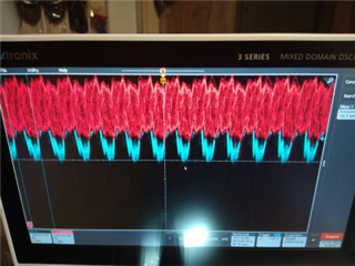
1) probing with an oscilloscope, we see (by eye) the outputs of LMK #2-5 to be in phase and of the same frequency (across all chips). However, the input and the output each are drifting against each other. Is that normal? "PLL" to me means the output is phase locked to the input, and both should be the same frequency or am I misunderstanding this?
2) A previous design used LMK010xx chips in stage 2 (LMK #2-5) instead of LMK03033, and X is only a little worse for 2 channels clocked by different LMKs. This follows the recommendation in the LMK03000 datasheet (8.9 MORE THAN EIGHT OUTPUTS ...). The LMK03033 was chosen here to have more flexibility in the final clock frequencies. Is the LMK03033 not suited for such a 2-stage architecture, only the LMK010xx?
3) The LMK03033 and LMK010xx being such similar devices, and if 2) is true, I am wondering if the LMK03033 can be programmed to act just like a LMK010xx? For example bypass the VCO stage and send the clock input directly to the output divider/delay stage; perhaps with register settings not listed in the data sheet? (I note some bits in e.g. register 9 are set differently for the two devices, but not explained)
Note: We are not overly concerned here with identical phase alignment of all the outputs (per the sync functionality). The phase can be different for different clock outputs, as long as that difference is _fixed_. A fixed phase offset will show up as a fixed offset from zero in the time measurement and can be calibrated out. Varying phase shifts worsen the precision X.