This thread has been locked.

If you have a related question, please click the "Ask a related question" button in the top right corner. The newly created question will be automatically linked to this question.

LMX2592: unstable PLL

Part Number: LMX2592

LMX2592_20MHz.zip

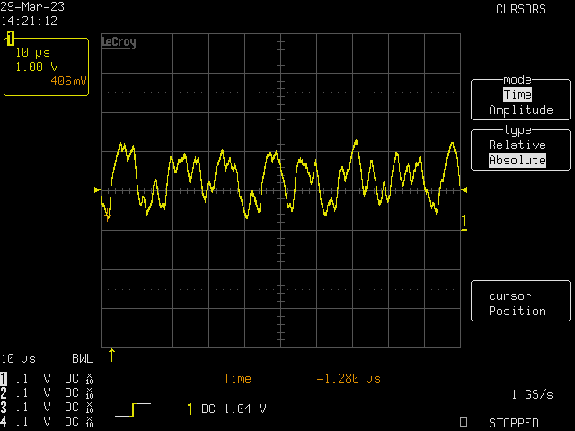
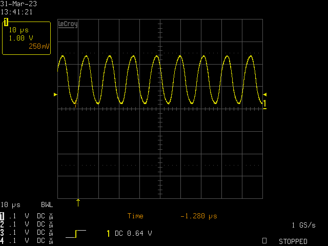
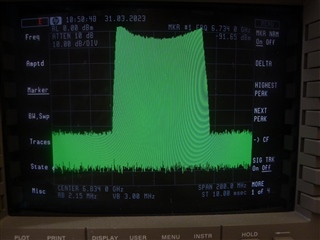
Dear Sirs,

I am having trouble getting stable PLL operation using the LMX2592. 

The following are the parameters:

reference frequency: 10MHz

Phase detector frequency: 20MHz

VCO frequency: 6.834682GHz

Integer divider: 170

Fractional modulus: 4000000000

Fractional numerator: 3468200000

I have programmed the registers to the Aug 2022 revision.

The output is centered around the correct frequency, however shows FM with a peak deviation of 40MHz. Looking at the tuning voltage on pin 35, a near sine wave is seen with a frequency of 87kHz, and an excursion from 0.2V to 2.3V.

The auto calibration is obviously working as the VCO is centered on the correct frequency.

I have taken the loop filter values from the Platinum Sim program, and the design is attached. I have checked the loop filter components.

I have tried different charge pump currents with no or little change.

I have tried setting the PFD_DLY parameter to 32 ( not used). This has a large effect on the tuning voltage. The sine wave is replaced by random noise. (Attached)

I have carefully checked the register readback for incorrect values, but may have missed something.

Please check the register dump for incorrect values

regards

Cosmo Little (RF Solutions)


REGISTERS.TXT

  • Hi Cosmo,

    Your loop filter has C3=150pF, this is not ideal. C3 should be placed close to Vtune pin and should has a value around 3nF.

    Your register setting use 15mA charge pump current while your sim file use 5mA. 

    You have set CP_ICOARSE to x2, this is not recommended anymore. If you really need 5mA, you don't need CP_ICOARSE.

    CAL_CLK_DIV should be set to 0x0, i.e. no division as your input clock frequency is low. 

    I tried your configuration on our EVM, I don't have any problem, loop filter remains as the EVM default value.

    How did you connect the 10MHz clock to LMX2592? Is it a square wave or sine wave clock? Isn't it a TCXO?

  • Dear Noel

    Thank you for your reply.

    1/- Value of C3. Using Platinum Sim, it is not possible to get a high loop bandwidth if C3 is set to 3nF. I want a loop bandwidth around 50kHz to minimise phase noise at 100Hz to 1kHz range.

    2/- I have changed CP_ICOARSE to 0, and have set all the CP_IDN and CP_IUP bits to give 4.8mA.  No effect on stability.

    3/-  I have set CAL_CLK_DIV to 0. No effect.

    4/- The reference is a 2Vpp sine wave from an OCXO. I have tried using an RF generator to provide the reference. The FM modulated output changes in frequency with a change in reference frequency, showing that the loop is locked , however with oscillation.

    5/- Attached RF output, and voltage on tuning pin.

    6/ We only have one sample of the LMX2592, as this part is absolutely unavailable to order at the moment. Could we have a couple of samples in case our un  it has a fault?

  • Hi Cosmo,

    Could you share your schematic showing how did you interface the OCXO to the device?

  • Attached schematic LMX2592

    We have a development board but had to remove the LMX2592 to transfer it to our prototype so we could test our own software. We cannot find any suppliers of the device. If you could possibly arrange some samples we could refit the development board and test our design on it, as well as on our own board.microwave_pcb_issue_1.10.pdf

    regards

    Cosmo Little

    PS do you have a list of DC voltages at the various decoupled pins of the chip?

  • Hi cosmo,

    I don't have the pin voltages in hand, this needs some lab work to get.

    If samples are not available to order in ti.com, you need to contact TI sales or customer support.

    Comment on your schematic. First of all, try put the 50Ω at reference clock input to see if that help. Next try change 1µF to 10µF. Make sure all the µF capacitors are at least X7R grade with low ESR. 

  • Dear Noel

    Problem found! An open circuit connection to one of the decoupled pins on the LMX2592.  This shows up the difficulty of using these packages for prototyping. As I said before, we had to lift the chip off a development board due to non availability ( except for some very suspicious far east suppliers) of the chip from usual suppliers. I am sorry to have wasted your time over this problem.

       I can now proceed with testing the feasibility of low rate FM by continuously writing to the fractional numerator. I have one question regarding the use of the FCAL_EN bit. After writing to the frequency registers, this bit is set to 1 to initiate the frequency calibration. I have noticed that this bit remains set. After a frequency change, I assume that it is not necessary to set the bit back to zero before writing a "1".  Could you please confirm this.

       If I clear the bit to "0", I assume that no calibration cycle will take place if I write to the fractional numerator, and do not write to the FCAL_EN bit. Could you confirm this. ( The FM deviation required is only a few hundred Hz, so no recalibration is needed)

    best regards

    Cosmo Little

    PS for best phase noise, the chip is very fussy regarding the level of the reference input. In our final design, we could use a square wave reference input. Is this advisable?

  • Hi Cosmo,

    whenever we program R0 with FCAL_EN=1, the VCO will calibrate. We don't need to toggle this bit 1 --> 0 --> 1. 

    After calibration and PLL lock, if you change the VCO frequency a little bit (say <10MHz), you could skip VCO calibration. Vtune is able to keep the VCO lock. In other words, after writing new fractional numerator value, you don't need to program R0. 

    PLL phase noise will be affected by the input clock slew rate. A 10MHz sine wave clock has very bad slew rate, right, square wave is recommended at this frequency.