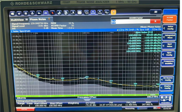
This thread has been locked.

If you have a related question, please click the "Ask a related question" button in the top right corner. The newly created question will be automatically linked to this question.

LMK04832: Regarding whether PLL is locked or not

Part Number: LMK04832


Tool/software:

To determine if the PLL is locked, I made the following settings:

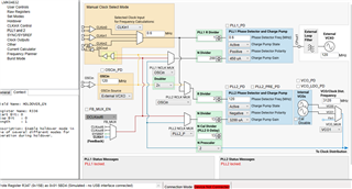
I want to observe the lock status of PLL1 and PLL2 through Status_LD1 and Status_LD2. 

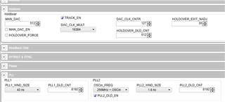
The configuration of PLL is as follows, using two PLLs at the same time and using a 120mHz VCXO externally:

Real machine testing has found that Status LD2 is high and Status LD1 is low.
When the external input clock source (600kHz) is turned off, there is no change in the status of Status LD2 and Status LD1.

As expected, when there is a clock input, Status LD2 and Status LD1 should be raised to indicate that PLL1 and PLL2 are locked. When there is no clock input, Status LD2 and Status LD1 should be low.

But that's not the case. May I ask where my configuration is problematic?

Also, I would like to ask if it is possible to use Status LD2 or Status LD1 to observe whether it is locked using only one PLL?

  • Assuming you are using the LMK04832EVM, here are some possible reasons:

    • Are you providing the clock input on CLKIN1 and selecting it on the CLKinX Control page? CLKin_SEL_MANUAL should be set to "CLKin1 Manual", and CLKin1_DEMUX should be set to PLL1. CLKin1_EN is not required to be set since this is only used for holdover clock selection.
    • Since you have holdover disabled, you may need to set CLKin_OVERRIDE=1 to ensure software selection of CLKIN1 always occurs. CLKin_OVERRIDE can be found on the User Controls page, in the General group at the top.
    • Does the slew rate of your 600kHz input source satisfy the minimum slew rate requirement of 0.15V/ns? This is frequently not the case with sine wave signal sources, where the maximum slew rate is 2π * f * Vpk. Square wave sources can usually satisfy this slew rate, but some low-frequency signal generators may have square wave slew rate limits below the required rate.
    • Is the VCXO a positive control voltage slope or a negative control voltage slope? PLL1 phase detector polarity may need to be flipped if the VCXO is a negative control voltage slope.
    • If the on-board VCXO is still present on the EVM, have you disabled it? The EVM will inject a 122.88MHz spur onto OSCin, which could interfere with the 120MHz external signal. You could solder a short from the enable pin on the VCXO to GND, or you could cut the power to the VCXO by desoldering the ferrite bead on the VCC network.
    • Is OSCout enabled? The 120MHz signal from CLKin2/OSCout, right next to the 600kHz signal, could be cross-talking to CLKin1. Set OSCout clock format to Powerdown on the CLKinX Control page or the Clock Outputs page; if OSCout is being used, make sure it's terminated off-board.
    • Similarly, you can also check the behavior of PLL1_R (and PLL1_N) on the STATUS_LDx outputs. You could route PLL1_R to one of the status pins, then check on an oscilloscope if the R-divider output signal is different from the CLKin1 signal.
    • What is the tuning range of the VCXO? The default EVM loop filter is designed for a high-performance 122.88MHz VCXO which has around ±25ppm/V gain (or around 3kHz/V). Since the loop stability depends on the VCXO gain, if a different VCXO has higher gain (e.g. ±50ppm/V or around 6kHz/V), this reduces the phase margin substantially with the same settings. If the VCXO gain of your 120MHz VCXO is not comparable to the gain used by the EVM default, the loop filter needs to be redesigned - PLLatinum Sim could help you with this.

    If you have a custom circuit design, and none of the applicable items above help, we could start looking for schematic or layout reasons.

  • Thanks for your reply:

    1. yes, i providing the clock input on CLKIN1 and selecting it on the CLKinX Control page. I removed CLKin1_EN and set CLKin_OVERRIDE to 1.

    2. I switched to a square wave clock source, and now PLL1 shows LOCKED (STATUS_LD1 is high).

    3.  the VCXO is a positive control voltage slope.

    4. It is a custom circuit design board without using the 122.88mhz VCXO

    5. CLKin2/OSCout has reserved a clock input option, but it is not currently being used

    6. Understood

    7 .--

    The current issue is that both PLL1 and PLL2 are locked.

    But when the input 600kHz clock is turned off, the lock signal of PLL1 is pulled low, while the lock signal of PLL2 is still high. Why hasn't the lock signal of PLL2 decreased at this time? Is the LOCK state of PLL2 correct?

    ##########################

    In addition, the Clock Output section is down converted to 240MHz and configured for LVDS mode output. IDL, ODL, DDC&HS are all checked.

    We tested CLKOUT2P/N (Use external balun to convert to single ended output during testing)  and found that the jitter performance was generally higher compared to the manual, especially in the range of 100Hz to 1KHz, which was significantly higher. Resulting in a final overall jitter of only 280fs. As shown in the following figure:

    May I ask if there are any other ways to reduce jitter?

    The design circuit diagram is as follows. Please check if there are any issues:

    20241218.pdf

  • But when the input 600kHz clock is turned off, the lock signal of PLL1 is pulled low, while the lock signal of PLL2 is still high. Why hasn't the lock signal of PLL2 decreased at this time? Is the LOCK state of PLL2 correct?

    The VCXO didn't stop oscillating just because PLL1 lost lock. The output frequency of the VCXO should be bounded to a narrow PPM range even when the control voltage is at the rail. Meanwhile, the VCO in PLL2 has a gain on the order of 30MHz/V. Using exaggerated PPM numbers for an example: even if the VCXO shifts by 100 PPM when PLL1 loses lock, that's a 12kHz reference frequency shift on a 120MHz VCXO; at 3120MHz, N/R = 26, so the VCO only shifts by 12kHz * 26 = 312kHz, which is only a 0.312/30 = 10.4mV shift in the tuning voltage at CPout2. In most cases, PLL2 will stay locked across the entire output frequency range of the VCXO.

    100Hz and 1kHz noise is close to the loop bandwidth of PLL1, so this is likely a result of the reference input noise summing with the PLL and VCXO noise before the reference noise is rolled off by PLL1 loop bandwidth. You could try further restricting PLL1 loop bandwidth, or increasing to a third order filter to more rapidly attenuate the reference noise contribution. You can simulate the effects of the loop filter in PLLatinum Sim. There are other posts on E2E that go into greater detail on how to simulate devices in PLLatinum Sim, including LMK04832 specifically. I can also offer specific guidance if needed.

    The noise floor is higher than what I would expect. I didn't see anything in the schematic that would cause increased noise floor. I do see that the signal level of the input to the FSWP is lower than I'd expect for LVDS through a balun (-4dBm). Are there long cables or other attenuating elements between the LMK04832 and the FSWP? Can this path be improved?

    The outputs appear to be AC-coupled to their targets. Can the format be changed to HSDS? This requires no component changes. If the receiver can accept a signal 1.5x larger than standard LVDS, HSDS 6mA improves the noise floor by 2dB over LVDS; if the receiver can accept a signal 2x larger than standard LVDS, HSDS 8mA improves the noise floor by 3dB over LVDS.

    I also see that the doubler and the R-divider are both enabled - I don't recommend this, because the doubler adds 0.5dB to 1dB noise to the PLL2 reference path. If you just want to use 120MHz phase detector, there is no benefit to enabling the doubler and the divider - just use divide-by-1 and set doubler to x1. You could also realize a modest performance improvement (about 2dB) between 10kHz and 100kHz offsets by using the doubler to increase the PFD frequency to 240MH - this requires some care on startup to handle the prime number N-divider, but it is possible with use of the FB_MUX:

    • On startup, the initial configuration should be for 120MHz phase detector.
      • Start with PLL2_R = 2 and the doubler set to 2x, as you currently are using it.
      • Start with N prescaler = 2 and PLL2_N_CAL = 13
    • Write PLL2_N = 1. VCO calibration is triggered by writing the LSBs of the N divider, which are in address 0x168. The PLL2_N_CAL value will be substituted into PLL2_N, the calibration will complete, then the PLL will restore the original N divider value and lose lock again. VCO calibration takes up to a few hundred µs to complete.
    • After calibration:
      • (optional) Disable subsequent VCO calibration by setting PLL2_FCAL_DIS=1. You should only do this if you expect to re-write the PLL2_N LSBs at some point.
      • Enable the FB_MUX and route a copy of CLKout6 or CLKout8 at 240MHz back to the FB_MUX.
      • Set PLL2_NCLK_MUX to use the FB_MUX as its source.
      • Disable the N prescaler path by setting PLL2_PRE_PD=1. This is necessary to reduce crosstalk.
      • Set PLL2_R=1. The PLL should now lock with 240MHz PFD.
  • Thank you for your suggestion. We are currently testing it.

    Well, there's another thing I'd like to ask.

    1. As the final device used can only provide sine waves, is there a similar chip that converts sine waves into square waves, or is there a chip with similar functionality to LMK04832, but without the minimum slim rate requirement of 0.15V/ns?

    2. Do you have any reference examples for PLLatinum Sim? Because there are too many parameters, I want to know what configurations can improve the quality of the final signal, and so on.

  • 1. We have some guidance on sine to square conversion, see https://www.ti.com/lit/an/snaa411/snaa411.pdf

    2. There's a few places I can suggest for different needs:

    General advice for improving phase noise:

    • Increasing the phase detector frequency of PLL2 decreases the in-band noise of the PLL by 3dB/octave. If a device allows increasing the phase detector frequency (e.g. doubler on PLL2 of LMK04832), and the frequency plan permits it, consider using the higher phase detector frequency.
    • Increasing the charge pump gain can improve the phase noise by improving the gain, but it also introduces additional noise due to the higher drive current and higher magnitude of uncorrelated current noise. Generally the improvement from increased bandwidth is beneficial enough to recommend it when possible, but PLL1 loop bandwidth may be low enough that the reduced gain does not greatly impact phase noise in the region of interest, allowing the charge pump gain to serve as a programmable loop bandwidth control instead.
    • Different output formats have different phase noise performance. LVDS has a higher noise floor contribution than HSDS, LVPECL, or CML; there may be system design tradeoffs involved (signal levels, DC vs AC coupling, etc) in output format selection that dictate using a noisier output format. Note that the output format displayed in PLL1 is for OSCout; the actual performance of the VCXO input into the OSCin buffer is usually much better.
    • The default loop filter suggested for PLL2 in LMK04832 is generally close to correct. In some cases, it can be beneficial to tweak the value of R2 or C2 to decrease the noise in one part of the loop at the expense of noise in another part of the loop.
    • When working with PLL1 + external VCXO simulation, I find it helpful to go to the phase noise tab and uncheck "Autoscale Axes", then set the X axis minimum to 1Hz and the Y axis maximum to 60dBc/Hz instead. Most of the PLLs in PLLatinum Sim target high-frequency PLLs with loop bandwidths in the 100s of kHz, but LMK04832 PLL1 is usually around 100Hz and may be off the plot when trying to investigate its behavior.
    • Generally there is no need for a loop filter greater than second order on PLL1, unless there are spurs on the reference that must be addressed. PLL2 only allows for controlling C1, R2, and C2 when using the internal VCO - other components are fixed.
    • The objective of PLL1 is to make the VCXO the primary contributor to phase noise above the loop bandwidth. A lower loop bandwidth tends to help with this. If the loop bandwidth is below 60Hz, I have seen some difficulties with rejecting AC line noise from radiated or conducted sources, so 100Hz tends to be about the sweet spot. There are a handful of cases where the VCXO performance is so good that the PLL needs to use a high phase detector frequency and a low charge pump gain to minimize additive noise contribution from the PLL.
    • In intermediate feature level and above, PLLatinum Sim can accept a comma-separated or tab-separated file with frequency offsets and phase noise values (you can check the expected format by using the data export features and inspecting those files). You can estimate the phase noise performance with a few points taken out of a VCXO datasheet, commit these to a file, and import these to PLLatinum Sim on the phase noise tab by selecting "Load Data" on the VCO noise radio button. Make sure to do this with the VCXO frequency and Kvco values set correctly, as subsequent changes to VCXO frequency will scale the noise to the new frequency. You can also do the same with the reference noise, if you know the reference noise characteristics.
    • PLLatinum Sim tries to auto-calculate the gain value of the VCXO (Kvco) in PLL1, but if you use a different VCXO than the EVM, you may want to substitute your own gain value. Disabling "Main Diagram Updates Performance Metrics" in the Options menu will disable recalculating the Kvco whenever the rest of the diagram changes.
    • On the Select Device page, there is an option to cascade the output of one device into the input of another device. This option appears to be broken in the latest version of PLLatinum Sim. You can work around this by exporting the total noise, selecting PLL2 with the desired VCO, and then loading the exported trace as a reference noise trace using the "Load Data" procedure described above.