This thread has been locked.

If you have a related question, please click the "Ask a related question" button in the top right corner. The newly created question will be automatically linked to this question.

Separate Output Supply pins on CDCx949


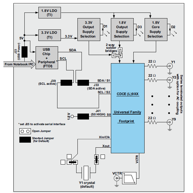
The datasheet as well as the general overview prominently lists that the CDCx949 has separate output supply pins (which is similar for most of the other CDCE clock synthesizers, like the CDCx937 or CDCx925), but I couldn't find any information which output supply pin (the CDCx949 has three of them) is correlated with each output (there are nine on the CDCx949).

Any information how they are related and/or where this information can be found would be truly appreciated.

Thanks in advance,

Herbert

  • Hi Herbert,

    I believe (but I am not sure) that "Separate Output Supply Pins" means that Vdd(out) is different from Vdd.
    As pins 3 and 13 must be the same voltage that is Vdd, also the pins 6.10 and 17 must be at the same voltage Vdd (out) that will be either 1.8, 2.5 or 3.3V (one voltage for all outputs) separately from Vdd that must be 1.8V.

    Regards,

    Mourad.

  • Hi,

    In CDCE(L)9xx Performance Evaluation Module, I find that for the outputs supply, a selection between 3.3V and 1.8V must be done.

  • Possible, leaves the questions:

    1. Are all pins internally connected?
    2. Do they need to be externally connected to VDDOUT?
    3. Is 1.8V on VDDOUT an option for the CDCE (non CDCEL) devices?

    Thanks,
    Herbert

  • Hi Herbert,

    If the pins have to receive different power supply, then they must be named, Vdd(out)1, Vdd(out)2, Vdd(out)3...

    All pins that have the same name have to be internally connected, and need to be externally connected to Vdd plane (for Vdd pins), to Vdd(out) plane (for Vdd(out) pins), and to GND plane (for GND pins).

    You can search in the internet for the purposes of multiple pins for power supply and for grounding in ICs...

    I believe that it is helpful in circuit layout and power supply decoupling: decoupling become harder as the current become higher, and having power supply multiple pins decrease the current per pin.

    Best Regards.

    Mourad

  • Agreed, but in a clock synthesizer, which produces a maximum of 12mA per output (typically way less) and consumes a total of 38mA for all PLLs active two Vdd pins, three Vddout pins and four GND pins seems a little excessive and I presume the actual reason isn't the enormous current draw.


    Looking at the entire CDCE(L) family, I think the main reason is some kind of footprint compatibility combined with some kind of pairing outputs in groups of two and shielding them with power or ground.

    But thanks for the input,
    Herbert

  • Ghorbel Mourad said:

    Hi Herbert,

    If the pins have to receive different power supply, then they must be named, Vdd(out)1, Vdd(out)2, Vdd(out)3...

    All pins that have the same name have to be internally connected, and need to be externally connected to Vdd plane (for Vdd pins), to Vdd(out) plane (for Vdd(out) pins), and to GND plane (for GND pins).

    You can search in the internet for the purposes of multiple pins for power supply and for grounding in ICs...

    I believe that it is helpful in circuit layout and power supply decoupling: decoupling become harder as the current become higher, and having power supply multiple pins decrease the current per pin.

    Best Regards.

    Mourad

    You are correct here Mourad. Internally, the Vddout pins are connected but do need to also be each connected externally. As you mentioned previously, this is a common tactic used for power supply decoupling - noise on supply planes can directly impact clock phase noise in a noticeable manner. It is safe practice to provide a good supply path to all Vddout and Vdd pins regardless of their internal connections.

    Gabe