

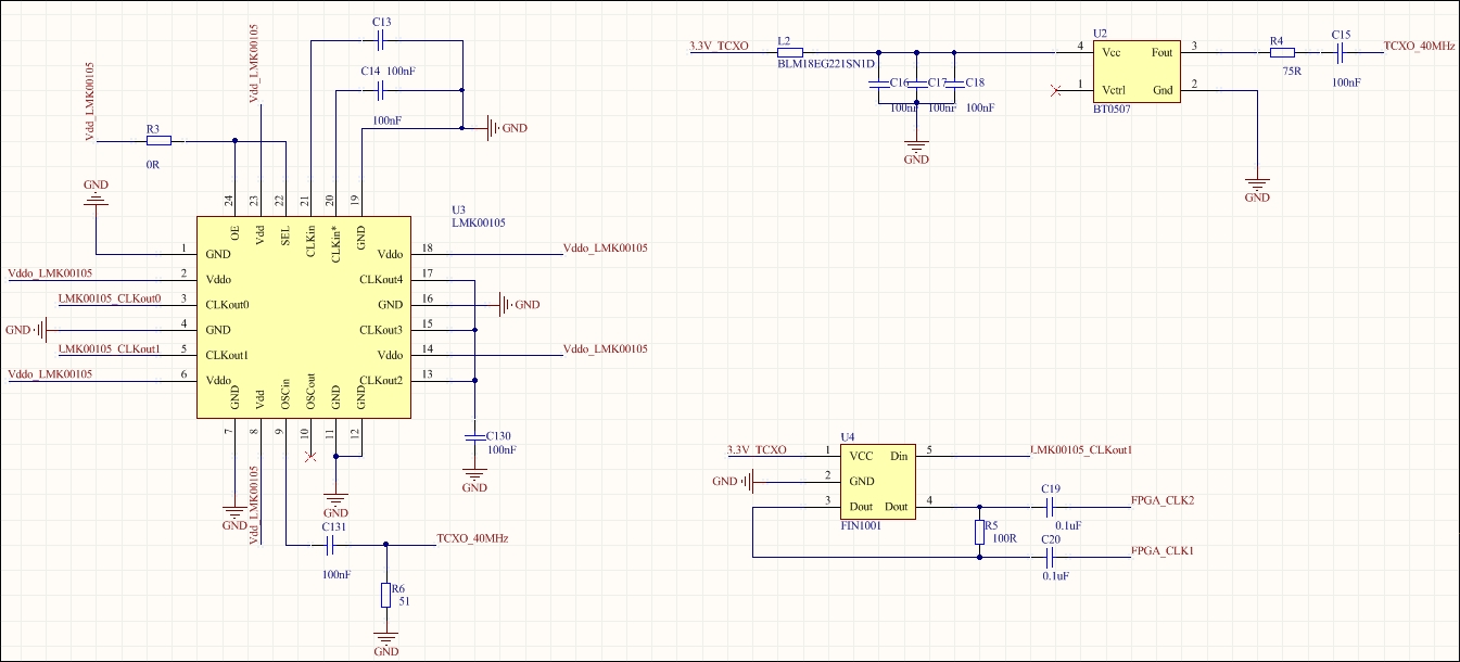
I plan to use a 50MHz TCXO as the source of the CLKin of LMK00105, the datasheet give that the input slew rate of the CLKin must be 2V/ns or more, but TCXO can't provide 2V/ns output, what should I do to meet the requirement on input slew rate?

-
Ask a related question
What is a related question?A related question is a question created from another question. When the related question is created, it will be automatically linked to the original question.

