This thread has been locked.

If you have a related question, please click the "Ask a related question" button in the top right corner. The newly created question will be automatically linked to this question.

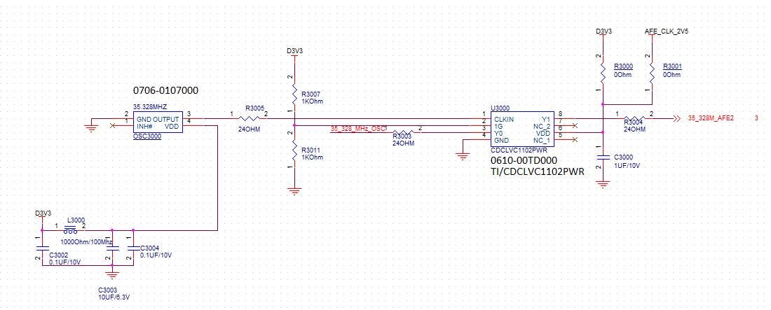
CDCLVC1102: Schematic review

Part Number: CDCLVC1102

Hi Sirs,

Sorry to bother you.

As title, could you help check our schematic?

The VDD will used +3.3V and to reserved LDO +2.5V,

Because we didn't find Pin 1G Output enable input voltage range from datasheet,is ok for our design?

Any suggestion is welcome.

Thanks!!

  • Hello Shu-Cheng,
    regarding your schematic:
    - 1G pin also follows VDD/2 threshold as the normal input. Therefore please add same option AFE_CLK_2V5 as you have on normal VDD pin for the pull-up R3007.
    - not sure how your supply isolation strategy looks like. It may make sense to put the buffer on the same isolated power as the oscillator. Please refer to Figure 13 of the data sheet for a decoupling suggestion.

    Best regards,
    Patrick