This thread has been locked.

If you have a related question, please click the "Ask a related question" button in the top right corner. The newly created question will be automatically linked to this question.

CDCLVP2108: Questions on CDCLVP2108RGZ IBIS model

Part Number: CDCLVP2108

Hi Experts,

There are couple of questions on CDCLVP2108RGZ IBIS model from customer, could you please help to comment? Thanks!

1. Name of comments and component is not aligned.

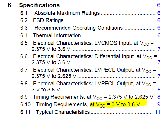
2. Voltage range is not correct. According to datasheet, "3V3" is from 3v to 3.6v,while in IBIS model it's from 2.375v to 3.6v.

 3. Lack of pull down curve.

4. There is no cross-zero point on GND clamp curve.

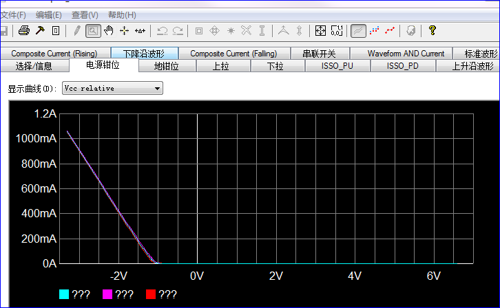
5.  For pull up curve, there is no data from -Vcc to 0, and for 0~Vcc, the curve should decrease smoothly.

 6. Power clamp current is too large, please help to confirm.


  • Hello Yuntao,

    Thanks for your interest in TI's product.

    We will look into your inquiry in more detail and get back to you. Meanwhile, many of the questions is based on visual inspection of the file. Do you have trouble simulating the model or have concerns regarding simulation results? The model is originated in 2009. So any detail info during your simulations will help us investigate.

    Thanks,

    Eric Kim  DSS/ADS/CAS 

  • Hi Eric,

    Is there any update? 

    Take below configuration for example, amplitude of SS is maximum and FF is minimum, in addition, the waveforms are in different starting point. 

    Thanks!

    BR

    Yuntao Yu

  • Hi Yuntao,


    Sorry I wasn’t able to get back to you sooner.


    Thanks for the waveform.

    It is not unusual to have a different starting point/level for different corners. I do see a proper trend where maximum coroner has the largest swing amplitude, followed by typical corner and min corner.


    Anyhow, to address your questions in the original post,

    1) The model file covers multiple devices, including “[Component] CDCLVP2108RGZ”

    2) Yes, it should’ve covered 3.0V as min corner instead of 2.375V. Unfortunately, the modell is quite old (original developer no longer with us) and it wouldn’t be easy at this time to add 3.0V corner model.

    3) Since the buffer is modeled as open_source, it is common not to have a pull down curve.

    4) and 5) considering this is a differential LVPECL driver in contrast to push-pull CMOS output, it is not usual to have this type of behavior.


    Hope this helps!


    Thanks,

    -Eric Kim DSS/ADS

  • correcting typo:

    4) and 5) considering this is a differential LVPECL driver in contrast to push-pull CMOS output, it is not UNUSUAL to have this type of behavior.
  • Hi Eric,

    Here I add customer's comments:

    1. Although the model file covers multiple devices, including “[Component] CDCLVP2108RGZ”, since the component and comments are not matched, could you update it?

    2. Since it should’ve covered 3.0V as min corner, and this device is widely used in customer's projects, is it possible to update it or is there any other method to evaluate 3.0V corner case?

    BR

    Yuntao Yu

  • Hi Yuntao,


    Thanks for the update.

    Regarding #1), it appears the customer is more concerned about “cosmetic” aspect of the model… We can certainly change/add additional component name. However, it wouldn't change the electrical behavior of the model. Anyway, I am not so certain about what the customer means by “the component and comments are not matched”. Can you please communicate with the customer what exact part number that the customer wants to see included? This will ensure we will eliminate unnecessary revisions in the future.

    2) This will be more challenging to implement. I believe the model on the web is approved by the product line. In order to initiate a new modeling work(at 3 V), I recommend you to contact the product line to submit a separate modeling request.


    Thanks,

    -Eric Kim DSS/ADS/CAS