This thread has been locked.

If you have a related question, please click the "Ask a related question" button in the top right corner. The newly created question will be automatically linked to this question.

LMK04133: Jitter clean up - LMK04133

Part Number: LMK04133
Other Parts Discussed in Thread: LMK03318

I'm currently working to resolve an issue with an existing design that seems to be related to clock jitter.  Specifically, I have a DLL in a video scaler ASSP that scales a reference clock to achieve different resolution timings, then that clock gets multiplied up by an FPGA DCM so the video data can be serialized.  By the end of all that, there appears to be enough jitter to cause the video to drop out occasionally.

I'm looking to improve this, and I'm considering either adding a jitter cleaner after the FPGA DCM or replacing it with a jitter attenuating clock multiplier IC.  The ratio in question is a fixed 1:7, and the input frequency can be anywhere from 20MHz to 150MHz (140MHz to 1.05GHz output).

I was looking at your LMK041xx family and experimenting with WEBENCH.  When I put an input frequency of 150MHz and an output of 1.05GHz, it narrowed the options down to the LMK04133 (though I'm not sure I understand why just that one).

I'm still reading and learning, but I was hoping I could get some advice as to if this part will do what I'm hoping, and if I should be using it to scale the clock too, or just clean jitter.

  • Do you know if the jitter from the FPGA DCM that causes the occasional video dropout is high-frequency jitter, low-frequency jitter, or both?  Have you tried to do jitter analysis/decomposition on the DCM clock that needs cleaning?  If you have some jitter analysis data on the DCM clock, could you share it?  Also, do you have the list of the different video clock frequencies/timings?  Is this for HDMI, SDI, or another video interface?  Some answers could help steer us towards a suitable clock device.  

    The LMK04133 (LMK041xx family) can clean both low and high frequency jitter, but you need to determine the external VCXO frequency, PLL N/R and Output divide ratios, and internal VCO frequencies (within the device's VCO tuning range) that can generate the required 7x multiplied clock and phase-lock to the different reference clock frequencies coming from the DCM.  Ideally, you can use a single ext. VCXO frequency to support all the different timings.  You could try the Clock Design Tool (www.ti.com/.../clockdesigntool) to search some of our Dual-Loop PLL jitter cleaners that may could the different timings you require.

    Alan

  • HDMI Device 1 Results 2018-08-28_17-35-43.mht.msgWe generate up to 4k 60Hz 4:4:4 HDMI 2.0 video, depending on the native timing of the attached monitor.  I've been working with the transmitter manufacturer, Explore Microelectronics, and their jitter analysis is attached; we're near 75pS of jitter on the 5.94Gbps output signal, and they believe the source of the excess jitter is the video data.  Our FPGA takes in a parallel LVTTL bus (120 bits) and converts it to FPD-Link LVDS (4 channel 5D+C), which gets converted to V-by-One HS LVDS (8 lane), before finally being transmitted as TMDS CML (8b/10b encoded).

    For the clock design tool, is the frequency for the VCXO its center frequency?

  • The scope jitter plots did not come through in the email you attached.

    For clock design tool, you enter the VCXO center frequency. After you select a dual-loop device (LMK04xxx device), you will be able to enter the VCXO's tuning gain sensitivity (in kHz/V).

    If the clock jitter component(s) that needs to be filtered is high frequency noise (above 1 MHz), then you could consider the LMK03318 clock generator/multiplier to filter incoming clock jitter above its programmable PLL bandwidth (typically set between 100~500 kHz).

    Alan
  • Thank you.  I will review your latest comments.  I will try to attach the file again.

    3301.HDMI Device 1 Results 2018-08-28_17-35-43.mht.msg

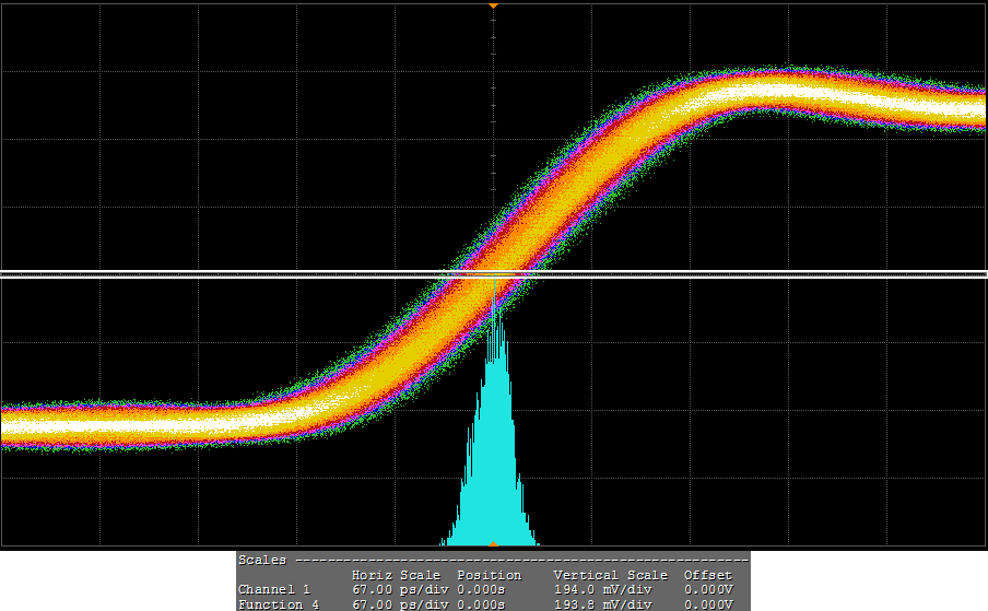
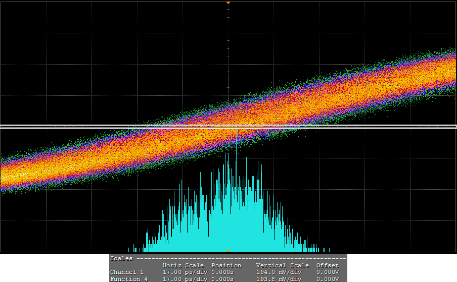
  • Okay, so just so I'm sure I understand, I tell the tool the VCXO center frequency and gain sensitivity, not the other way around?  If not from the tool, how do I determine these?  (Jitter plots are below.)

  • The external VCXO's min. gain sensitivity parameter, Kv (in kHz/V), of the can be estimated by:

    Kvco = f_vcxo * [+APR_ppm - (-APR_ppm)] / (Vc_high - Vc_low)

    where:

    • f_vcxo = VCXO frequency (in MHz)
    • +APR_ppm = upper range of minimum absolute pull range spec (in ppm)
    • -APR_ppm = lower range of min. absolute pull range spec (in ppm)
    • Vc_high = control voltage input high level (in V)
    • Vc_low = control voltage input low level (in V)

    Regarding the jitter histogram plots you sent, this does not capture the frequency of the various jitter components.

    Alan