This thread has been locked.

If you have a related question, please click the "Ask a related question" button in the top right corner. The newly created question will be automatically linked to this question.

LMK04828: output terminations resistors connections for LVDS outputs

Part Number: LMK04828
Other Parts Discussed in Thread: ADC12DJ3200, TIDA-01028

Hi TI,

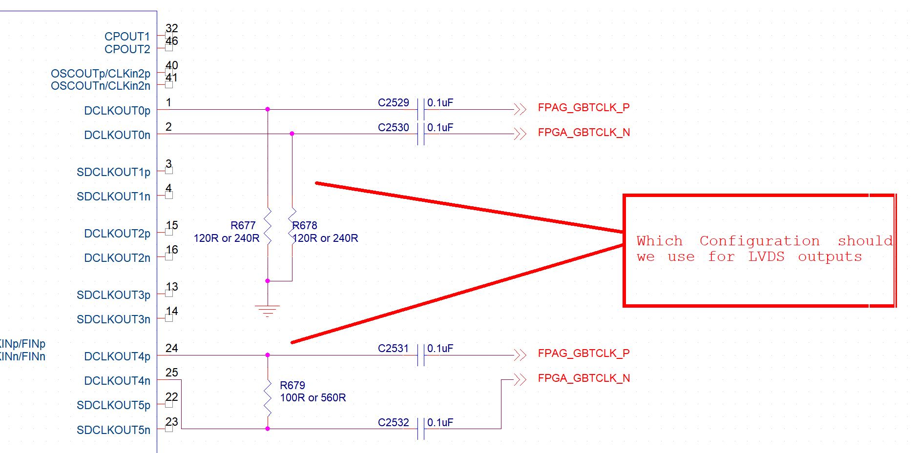
We will be using LMK04828 for generating Sysref clocks for ADC12DJ3200 and for generating GBTCLK,Sysref clock and Referenc clock for virtex-7 FPGA.

Now ADC12DJ3200 sysref clock standard is LVPECL so I will be using 120 Ohm pull down resistor on both P and N outputs of LMK04828.

But FPGA clocks (GBTCLK,SYSREF and REFCLK) will be using LVDS standard.

So which configuration should we use for LVDS outputs from LMK04828 from the below schematic:

Also , we have seen the schematic of TIDA-01028 in which two ADC12DJ2300 are used.

In this schematic, LMK04828 outputs used for FPGA clocks use 240 pull down resistor as termination. We are assuming TIDA-01028, also generate LVDS outputs from LMK04828 for FPGA.

So can LMK04828 generate LVDS outputs, even though outputs are terminated with 120 or 240 Ohm pull down resistors instead of shunt 560 or 100 Ohm resistors.

An early response will be highly appreciated.

Thanks,

Lalit

  • Hi Lalit,

    For LVDS, the configuration on DCLKOUT4 looks like the best option. The configuration on DCLKOUT0 is for LVPECL or LCPECL.

    If the FPGA has internal 100Ω differential termination, R679 should be 560Ω. If the FPGA is unterminated, R679 should be 100Ω and should be placed close to the FPGA (along with the AC coupling capacitors). Note that in order for the LVDS buffer circuit in the LMK04828 to power up correctly, there needs to be a DC path for current between the OUTP and OUTN terminals on the output. 560Ω is found to work well for the DC path.

    In TIDA-01028, it looks like 240Ω pull downs are used both as an emitter resistor for LVPECL, and in a few cases as a divider to reduce the signal voltage for interfacing with downstream devices. LVPECL 1.6Vpp differential signal levels with 240Ω emitter resistors should be able to directly interface with the FPGA's 1.8V I/O - see table 19 of the Arria 10 datasheet.

    That being said, if LVDS is desired, it should be possible to use the DCLKOUT4 configuration in the image above, and change the output buffer format on the LMK04828 to LVDS.

    Regards,