


Dear engineer !
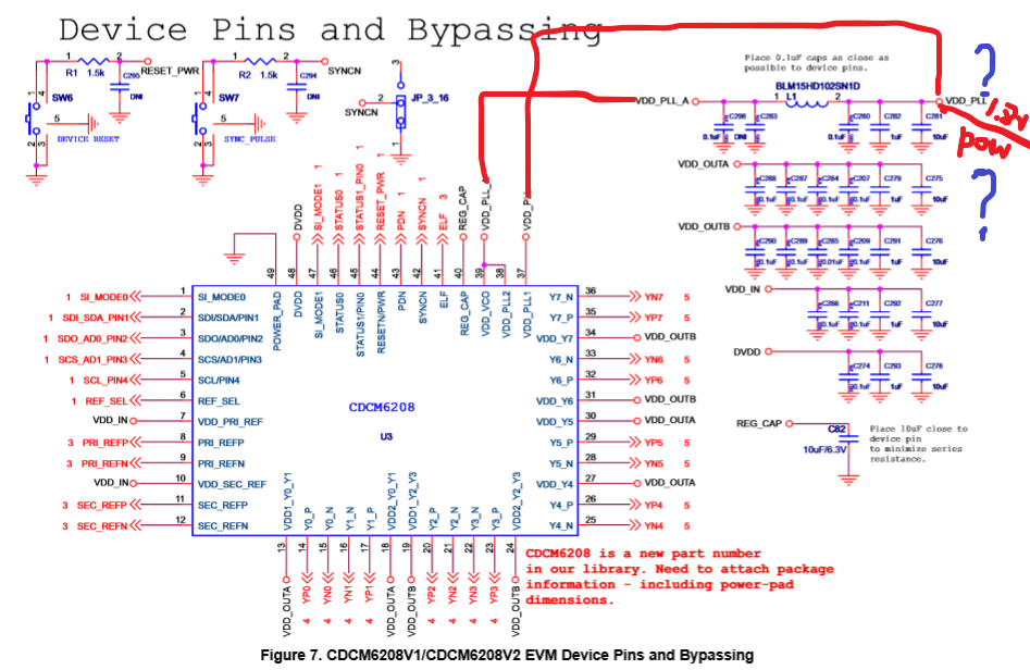
Recently I am looking at the CDCM6208EVM file. I have two questions about the schematic diagram of the file
1.as shown in the figure, Is this pin connected as shown in the picture and then the external power supply is connected to the VDD_PLL pin and so is VDD_OUTA/B?
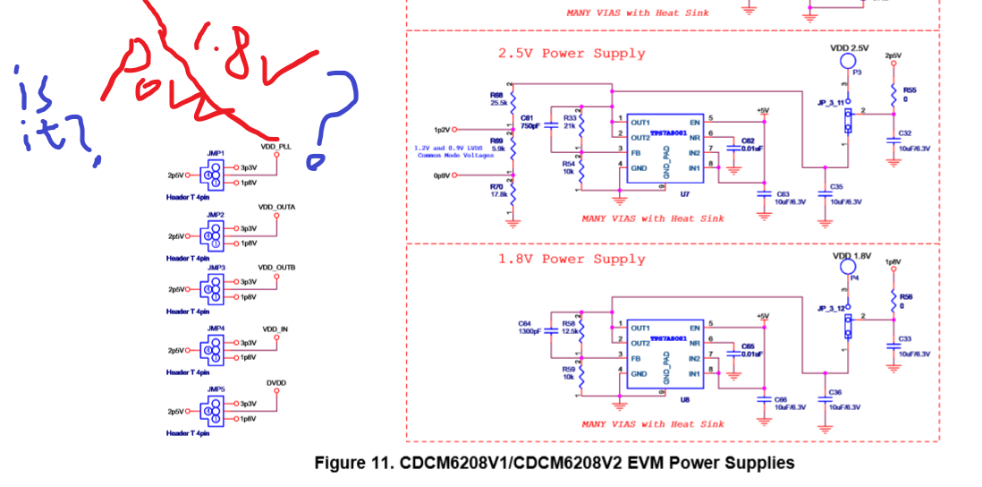
2.In order to save PCB board space, can I use only one power chip(TPS7A8001) to output 1.8v to VDD_SEC, VDD_VCO, VDD_PLL1 and VDD_OUTA at the same time?
Thanks
