Other Parts Discussed in Thread: DAC3282
Hi Texas Team
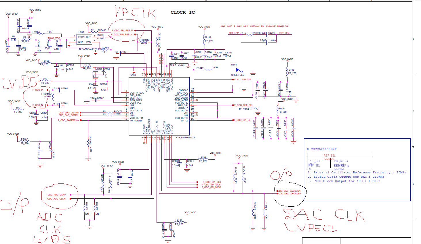
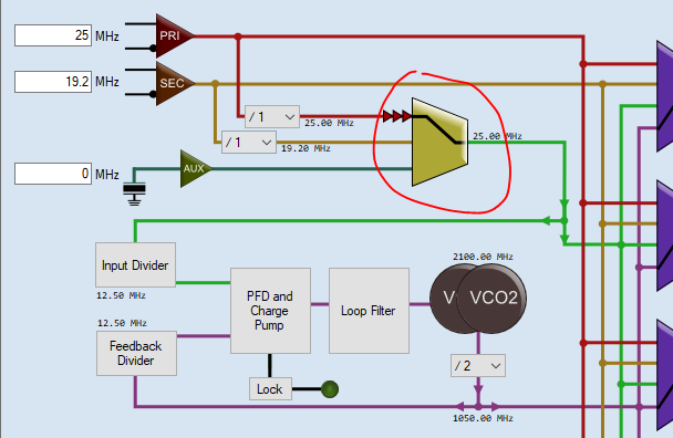
We are using CDCE62005RGZT in our design. The primary reference clock is 25MHz which coming from FPGA. We have also given the option for a secondary reference clock from a crystal oscillator TXETCLSANF-25.000000. We are not using output channel 1(U0N, U0P). Output channel (U1N, U1P)for DAC3282 @LVPECL clock 210 MHZ.Output channel (U2N, U2P)for ADS5482IRGCT@LVDS clock 105 MHZ.Output channel (U4N, U4P)for Xilinx FPGA @lvds clock 105 MHZ.What is the design issue we have to take care of? And what is the register value for PLL lock? I am finding it very difficult to generate register value from the software tool. Can u provide that? I need the Register value for both Manual mode and automotive mode. I have tried from software but the PLL lock issue still there. I am attaching the schematics file for detailed review. Please suggest any valuable review points in the schematics file.
Thanks and Regards
Balvan Singh
R&D Engineer(Hardware)
Phone: 918683919824