This thread has been locked.

If you have a related question, please click the "Ask a related question" button in the top right corner. The newly created question will be automatically linked to this question.

LMK04906BEVAL: OSCin voltage input range violated?

Part Number: LMK04906BEVAL
Other Parts Discussed in Thread: LMK04906, LMK04816BEVAL

Hi,

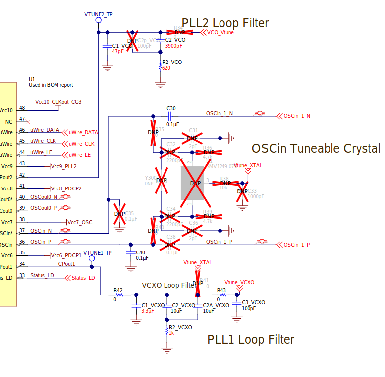
We noticed in the schematics of the LMK04906BEVAL that the 3.3V LVCMOS reference crystal oscillator (U2) is coupled using a 0.1uF dc-blocking capacitor into one of the OSCin inputs (the other OSCin input being connected to ground also using a 0.1uF capacitor).

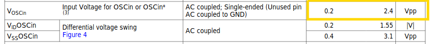
In my eyes this violates the maximum input voltage on the OSCin pins as given in the datasheet (page 7) V_OSCin: 0.2 to 2.4 Vpp. Can you clarify?

We need to know how we can connect our 3.3V LVCMOS oscillator to the OSCin pin and whether we need to use some kind of signal attenuation.

Best Regards and Thanks!

  • Hello Simon,

    The OSCin termination in the LMK04906BEVAL schematic is for a single-ended AC coupled input termination. A single-ended AC-coupled input termination was also used to measure the V_OSCin. Since both cases are AC coupled, the maximum input voltage for both cases will be the same (0.2 Vpp to 2.4 Vpp).

    For a 3.3 V LVCMOS oscillator input, there are two possible terminations.

    The first is to AC couple the input. This is done by placing a 0.1 uF capacitor on between the OSCin pin and the LVCMOS oscillator output and tying the OSCin* to ground through a 0.1 uF capacitor (as shown below in figure 24). Please note that although it says CLKinX/CLKinX*, this figure is also accurate for the OSCin/OSCin* pins.

    The second termination type is to DC couple the input. This is done by connecting the OSCin input directly to the LVCMOS oscillator output and tying the OSCin* pin to ground through a 0.1 uF capacitor (as shown below in figure 25). Please note that although it says CLKinX/CLKinX*, this figure is also accurate for the OSCin/OSCin* pins.

    Regards,

    Kia Rahbar

  • Hello Kia,

    Thank you for your thorough reply!

    Interestingly, the schematic of the LMK04906BEVAL does not exactly use either of those methods. It uses just a single DC-Block and no resistors in the path.

    Below the figures 24 and 25 from the Datasheet of the LMK04906 that you have shown it says:

    The voltage swing at the inputs must meet the specifications for AC coupled bipolar mode clock inputs given in the table of Electrical Characteristics. In this case, some attenuation of the clock input level may be required.

    The table of Electrical Characteristics says:

    This leads me to the conclusion, that the LMK04906B OSCin input is overdriven by the VG-4231CA CMOS output which violates the V_OSCin specification of 2.4 Vpp max.

    Interestingly, I looked at the LMK04816BEVAL board and it also uses a CMOS VCXO (CVHD-950) however in contrast to the above shown LMK04906BEVAL a voltage divider of 100R/51R is implemented which limits the voltage swing to 1.1Vpp.

    This leads me to the conclusion that the LMK04906BEVAL might not be correct in connecting the VCXO to the OSCin input and that I should rather follow the route of the LMK04816BEVAL.

    Best Regards

    Simon

  • Hello Simon,

    The voltage divider is only necessary if the input voltage from the oscillator has a swing greater than 2.4 Vpp. Depending on your system, you may require the addition of a voltage divider to attenuate the OSCin signal. On the LMK04906BEVAL, we do not include any voltage dividers as the necessary values would depend on each users system.

    Regards,

    Kia Rahbar