This thread has been locked.

If you have a related question, please click the "Ask a related question" button in the top right corner. The newly created question will be automatically linked to this question.

LMX2491: Start-up time

Part Number: LMX2491

Hi everyone,

I'm working with the LMX2491 PLL at the moment. Recently some problem came up and I was wondering if it has something to do with the start-up procedure of this component but unfortunately, there are no information about the start-up and/or enable times given in the datasheet. 

Some more details:
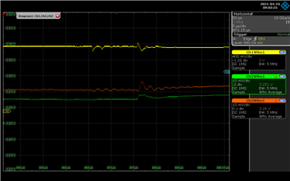
We are using the LMX2491 for an FMCW radar application but see some disturbance on our IF signals. Further investigations showed that these are also visible in the tuning voltage of the VCO, measured at the CPout pin, as can be seen in the scope screen shot below (green curve = tuning voltage, yellow curve = IF signal).

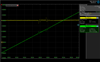
These disturbances appear always at the same time (between 800 µs and 900 µs after the PLL is switched on, varying between exemplars but fixed for one specific). The supply voltage is clean at that time.

For better understanding: We are powering the PLL (or rather the whole RF circuitry) only for short periods. After powering it up the system waits for a PLL lock signal and starts the ramp. After one ramp is sent the system is powered down (Vcc is switched off).

If the PLL is powered continuously, the disturbance only occurs once after the stat-up.
These results led us to the conclusion that there is something happening within the PLL itself. Has anybody some intuition if this could be possible? Is there probably still some start up process going on? Or is there some information about the start-up time of the device?

Thanks, and best regards

Chris

  • Hi Chris,

    My coworker will get back to you next Monday.

    Regards,
    Hao

  • Hi Chris,

    I don't aware if there is any "timer" in the chip that would be possibly causing this issue. 

    What happen if you wait a few ms, after lock detect has asserted HIGH, before starting the ramp?

    Will it make any difference if you power up/down the PLL via the CE pin instead of doing a Vcc power cycling?

  • Hi Noel,

    thank you for your fast reply. 

    If I add a delay after the PLL lock then the ramp itself is clean, as well as the IF signal. But the same disturbances on the CPout signal appear now in the time between the PLL lock signal and the start of the ramp (i.e. the added delay time), again at about 850 µs after turning the power on.

    However, if the PLL is powered continuously and only the CE pin is switched no disturbances appear. The problem with this is, that we don't have enough energy to power the PLL permanently (not even in Power Down Mode).

  • Hi Chris,

    I don't have any idea, let me check with the team and get back later.

  • Hi Chris,

    I checked with the designer, we confirm that there is no any kind of "timer" in the chip that would be causing disturbance at a fixed time.

    One possibility is, there is an external interference at this particular time period. It could be an interference to the VCO or there is some SPI transaction (if the SPI is shared between the PLL and other devices) during this time. Could you check?

  • Hi Noel,

    thank you for your answer and sorry for my late reply to it. I had a few days off and was busy with another project.
    But now I checked the signals around the VCO, and there seems to be no external interference. The SPI bus is only used by the PLL and the microcontroller, and there is no communication going on at that time.

    However, I measured several PLL-internal signals by switching them to the MUXout pin, and the Charge Pump Up Pulse (CPUP) drops significantly (green curve in scope screen) during the time of the interference. The supply voltage (orange/red curve) is stable during that time. The yellow curve is, as in my first post, the IF signal.

    I already tried to modify the loop filter, but the interference does not change (or at least not significantly). And it appears in ramp mode as well as in CW mode.

  • Hi Chris,

    I will check with the designer on the CPUP.

    The orange trace shown above is not a flat trace, isn't it a measurement issue or it is related to the issue? Which supply pin voltage it is? Can you also probe Vcp pin?

  • Hi Noel,

    Thank you for taking so much care.

    Yes, you’re right. The orange curve is not completely flat during the entire measurement, but since it shows the largest disturbance at the end of the interference, I concluded that this is just an effect but not the cause. The small ripple on the VCC at the beginning of the interference (between 865 µs and 870 µs) are pretty small (< 2 mV), so I don’t think that they cause such interference, or is the device that sensitive?

    The VCC depicted in my previous post is measured at pins 18 and 19 (delta-sigma engine and general circuit) and, while I’m not powering these pins continuously, the interference appears, no matter if the rest of the PLL’s VCCs (pins 7, 8, and 22) are powered permanently or switched.


    I checked the VCP pin (orange curve), and it also shows some disturbance, but at the beginning of the interference, it is also pretty small (< 2mV). We use ferrite beads at the VCC pins, and the shown signals are measured directly at the PLL. If I measure the supply voltage before those beads, only the latter disturbance is visible but smaller (see green curve).

  • Hi Chris,

    Please try set R2[3] = 1, this will disable some logic routine from running. This routine will complete in 130µs after POR, it should not be this routine that leading to your issue, simply give it a trial to verify. 

  • Hi Noel,
    great, this works. Thank you very much. After writing R2[3] to 1, the interference on the CPout signal vanishes, and therefore also the IF signal is clear.
    Does disabling this routine have any side effects (for my application), or can I safely do this?

  • Hi Chris,

    I am asking the designer for this, stay tuned. 

  • Hi Chris,

    That logic routine is required, we are looking into a workaround.

    Would you do me a favor to read back register R40 to R57, R143 and R144 after a Vcc power up? Thank you.

  • Hi Noel,
    Thank you for working on that.
    I will try to provide you with the register values tomorrow.

  • Hi Noel,

    here are the read back values of the registers you asked for:
    R40 - 0x00
    R41 - 0x00
    R42 - 0x00
    R43 - 0x00
    R44 - 0x00
    R45 - 0x00
    R46 - 0x40
    R47 - 0x40
    R48 - 0x00
    R49 - 0xA0
    R50 - 0x00
    R51 - 0x00
    R52 - 0x80
    R53 - 0x00
    R54 - 0x80
    R55 - 0x40
    R56 - 0x00
    R57 - 0x00

    R143 - 0xA0
    R144 - 0x00

  • Hi Chris,

    If we skip the logic routine, we expect the loop bandwidth will have 5 to 10% variation from the original. Spurs may be a little bit higher than before. Please verify if these deviation will affect your system.

    We can manually fix this deviation:

    Write R142 = 0x80 (if it is same as POR default value, then this step can be skipped)

    Write R54 = 0x60

    Write R55 = 0x60

  • Thank you for your help Noel. I think this works for us.