This thread has been locked.

If you have a related question, please click the "Ask a related question" button in the top right corner. The newly created question will be automatically linked to this question.

ADS127L01:

Part Number: ADS127L01

We run three of these ADCs in sync with each other, on the same CLK signal. Picture 1 shows how each ADC is wired (they are all identical). Strange intermittent readings from the ADCs were what started me on this investigation. Every once in a while, one of the ADCs would produce a reading that I would not expect to see. Throughout my investigation, I found that the DRDY pins of the ADCs get "knocked out of sync." By saying that I mean that the DRDY lines of each ADC will go low at the same time and in sync like they should (picture 2) , until something triggers them to go low about 80ns from each other. The trigger then happens again and they are now 120ns apart (the actual time increment is not important here, just the fact that the DRDY lines get out of sync). This process repeats and the DRDY lines get further and further from each other. Picture 3 shows the DRDY signals from two ADCs out of sync.

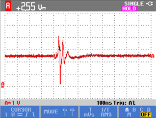
What I have found, and what my team and I believe to be the "out of sync trigger", is a transient voltage spike/dip on the VREFP line. It lasts for around 100ns, spikes the reference voltage past the chip's max voltage limit, and dips pretty low as well. Picture 4 is an example of this VREF transient. We are currently trying to get rid of this transient, but I would still like to get an understanding of your chip and it's synchronization quirks, to know if my theory could be true.

* The VREFP voltage in our circuit is 2.5V, and the transient spikes up to almost 4V. The max voltage on the VREFP line is 3.3V as per the datasheet. Could this violation cause the ADCs to lose their synchronization?

* The transient also dips the VREF voltage to almost 1V, could this be causing the ADCs to somehow reset, therefore losing their sync?

* Could these strange readings be a symptom of the Out-of_range system monitor from section 8.3.5 of the datasheet instead of synchronization loss?


Whatever the cause of this out-of-sync event is, I have found a 'band-aid' solution with software. By periodically taking the start pin of all 3 ADCs low and then high again, the DRDY signals snap back in sync. The out of sync trigger event still happens, and the DRDY signals still periodically get out of sync from it, but they snap back into synchronization before any problems arise. This solution was found by reading section 8.4.3 of the datasheet, and I made sure the timing requirement tw(STL) is satisfied from table 13.

With this band-aid in place, the ADCs can run for many hours without producing any strange readings. I have yet to see any strange readings thus far.

  • Hello Jonas,

    Welcome to the TI E2E Community!

    Regarding your first question, yes it is possible.  Exceeding the maximum input voltage on the REFP pin could cause the digital logic to upset, but it really depends on how much current is forced into the pin due to the transient.  The internal ESD diodes will turn on, and route most of the current to the AVDD supply pin, but if enough current is forced through the internal ESD diodes, some current may find another path inside the IC, which could cause the internal logic to glitch.

    For your second question, as long as the reference voltage is within the supply rails (greater than 0V or less than AVDD), you will not see any glitches in the operation of the device, other than the noise on the reference input showing up in the conversion readings.

    If the inputs over-range, as long as the input voltages and the reference voltage stay within the supply rails, you will not see any issue with the digital function, including the synchronization.

    Looking at your schematic, I see that you use two different ground symbols for analog and digital grounds.  It is important that the ground pins on the ADS127L01 are connected to the same ground plane near the device.  If these pins are connected to separate ground planes that are joined several cm's away, this can definitely cause glitches in the behavior of the device.  It is not uncommon for a transient to cause several 100's of mV of transients between analog and ground planes, and if this exceeds the ABS max level of the ADS127L01, +/-300mV, you will likely see hiccups in the operation of the device.

    Using the START pin to re-establish synchronization is the recommended approach. Since you are seeing fixed jumps in the timing between /DRDY pins, the ADC input CLK pins are likely clocking transient noise on some of the ADC's, which is causing the loss in synchronization.

    Regards,
    Keith Nicholas
    Precision ADC Applications

  • Keith,

    Thank you for your detailed response. My team and I are testing out your comment on different grounds, because we are definitely violating the "several cm's away" rule. Apparently this was a thought out and discussed decision by the hardware design folks, but this seems to be the first symptom we are experiencing from it. 

    With our current circuit design, it's not so easy to short the two ground planes near each device. Like I mentioned earlier, we have three of these ADCs, each on a small circuit board that plugs into a main circuit board (where the AGND and DGND planes are connected), and we have many other ADCs and DACs that have similar requirements. We obviously need to meet this criteria for our ADCs to work properly, but our analog and digital grounds are connected in one place for a reason.

    Do you have any general guidelines when it comes to best meeting the "less than several cm's away" rule when your design has multiple ADCs and DACs on small circuit boards?

    Best,

    Jonas

  • Hi Jonas,

    In general, with the ADC evaluation boards, we typically use a single ground plane and partition the components around the ADC to avoid digital currents flowing through the same section of the ground plane as the analog currents.  As you correctly point out, this becomes much more complex with multiple data converters on the same board, or in the same system.  In general, if you have separate analog and digital ground planes on your board, then you should treat the AGND and DGND pins on the ADC as analog grounds, and connect both to the analog ground plane.  In this case, some digital current will flow in the analog ground, but it will only be the digital current for the ADC, which is much lower than the digital currents in the processor section of the board.

    Please take a look at this e2e post that goes into more detail on this subject.

    https://e2e.ti.com/support/data-converters-group/data-converters/f/data-converters-forum/755516/faq-pcb-layout-guidelines-and-grounding-recommendations-for-high-resolution-adcs

    Regards,
    Keith