This thread has been locked.

If you have a related question, please click the "Ask a related question" button in the top right corner. The newly created question will be automatically linked to this question.

ADS8556: AGND and BGND connection on Layout

Part Number: ADS8556
Other Parts Discussed in Thread: ADS8586S

Hi Team,

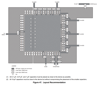
Could you tell me any important note on AGND and BGND connection ADS8556's layout?

It looks AGND and BGND are connected on simple plane under device on top layer though, I can not see the plane of EVM layout of ADS8556. So I'm a little bit confused how we should do. 

Regards,

Takashi Onawa

  • Hi Takashi,

    Splitting ground is not easy for customers to achieve the best performance, and a solid ground plane will be easier. This is the reason why a single ground plane is commonly designed on all new EVMs including the new ADS8555EVM-PDK which supports to evaluate ADS8556 as well.

    Also, ADS8586S is the latest 6-ch/16-bit simultaneous-sampling ADC which has more features and benefits for customers including a single power supply and high input impedance(1Mohm) etc. Note that ADS8586S has integrated a LPF filter on each channel.

    Best regards,

    Dale

  • Hi Dale-san,

    Thanks for your prompt response on this but I was confused more...

    Do you recommend to be connected to simple GND plane for all AGND and DGND pins? Or should refer to the recommended layout on datasheet?

    On the datasheet recommendation, DGND and AGND is split on GND layer. And I can not see all layer on ADS8555EVM's layout.
    Can you easily draw a diagram of the recommended layout? Or share the EVM full layer layout file?

    Regards,

    Takashi Onawa

  • Hi Takashi-san,

    A simple and solid ground plane is recommended for all AGND and DGND pins. On the ADS8555EVM, the 2nd layer is the GND plane and all AGND and DGND pins are directly connected to this layer with via holes. 

    Regards,

    Dale

  • Hi Dale-san,

    Thanks for your comments, They understood that TI recommend Non split GND plan for the design but could you share the raw layout file of the EVM?
    They want to refer it for their design but it is difficult to see the detail of full layer information from its pdf user's guide.

    Regards,

    Takashi Onawa

  • Hi Takashi-san,

    The EVM used the entire 2nd layer for GND. nothing is special. I can review your customer's sch and layout if they can share them to me.

    Best regards,

    Dale