I'm getting both an inconsistent and unexpected result when writing and reading to registers on my ADS1299.
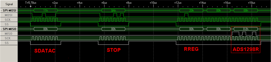
I start up the ADS by resetting by sending the command RESET (0x06). I then use the command SDATAC (0x11).
Using RREG (0x20) and reading from register CONFIG1 (0x01) to CONFIG4 (0x17), I get the expected result as stated in the datasheet.
| TX comment | RESET | SDATAC | RREG + 0x01 | 16(+1) registers | |||||||||||||||
| TX | 06 | 11 | 21 | 16 | 00 | 00 | 00 | 00 | 00 | 00 | 00 | 00 | 00 | 00 | 00 | 00 | 00 | 00 | etc. |
| RX | 00 | 3C | E0 | 00 | 00 | 96 | C0 | 60 | 00 | 61 | 61 | 61 | 61 | 61 | 61 | 61 | 61 | 00 | etc. |
| RTX comment | CONFIG1 | CONFIG2 | CONFIG3 | CH1SET | CH2SET | CH3SET | CH4SET | CH5SET | CH6SET | CH7SET | CH8SET | BIAS_SENSP |
When writing to register (WREG) CH1SET and setting it to e.g 0xF6 (which should be valid) and then reading (RREG) the registers again, I get
| TX comment | RESET | SDATAC | WREG + CH1SET_addr | 0 (+1) registers to write | Write value | SDATAC | RREG + CONFIG1_addr | 16 (+1) registers to read | |||||||||||
| TX | 06 | 11 | 45 | 00 | B6 | 11 | 21 | 16 | 00 | 00 | 00 | 00 | 00 | 00 | 00 | 00 | 00 | 00 | etc. |
| RX | 00 | 00 | E0 | 00 | 00 | 7F | FE | 47 | FF | 96 | C0 | 60 | 00 | 7F | 61 | 61 | 61 | 0061 | etc. |
| RX comment | ? | ? | ? | ? | CONFIG1 | CONFIG2 | CONFIG3 | LOFF | CH1SET | CH2SET | CH3SET | CH4SET | CH5SET |
Notice that CH1SET gets the wrong value. However if I try to set CH1SET to 0x20 (which shouldn't be valid since a couple of the bits are reserved?), RREG shows correct result.
Also, often the ADS gives even more wrong values that aren't close to correct. Below is the same commands as above, but with an entirely different outcome.
| TX comment | RESET | SDATAC | WREG + CH1SET_addr | 0 (+1) registers to write | Write value | SDATAC | RREG + CONFIG1_addr | 16 (+1) registers to read | |||||||||||
| TX | 06 | 11 | 45 | 00 | B6 | 11 | 21 | 16 | 00 | 00 | 00 | 00 | 00 | 00 | 00 | 00 | 00 | 00 | etc. |
| RX | 00 | 00 | E0 | 00 | 00 | 7F | FE | 3F | FF | 00 | 00 | 00 | 0F | 00 | 00 | 00 | 00 | 00 | etc. |
| RX comment | ? | ? | ? | ? | CONFIG1 | CONFIG2 | CONFIG3 | LOFF | CH1SET | CH2SET | CH3SET | CH4SET | CH5SET |
My best guess is that it would be some error related to timing. I read somewhere that timing issues could cause errors when reading registers.
Trying to write to both CH1SET and CH2SET gives even more odd values. For example if I set CH1SET = 0x20 and CH2SET = 0x30, I get this result.
| TX | ||||
| RX | 20 | 61 | 30 | 61 |
| RX comment | CH1SET | CH2SET | CH3SET | CH4SET |
CH2SET and CH3SET seem to have been switched. I've double and tripled checked the values that I send.
How important are the timings that are explained in the datasheet? In a multibyte-command, instead of waiting exactly <1.46µs between tx, coud I wait 1 ms or could this cause issues?
If you have any idea what I could be doing wrong, or what I could do to narrow my search for the source of the issue, I'd appreciate the help.
Thank you in advance!
Some relevant code
ADS_Transmit(&(uint8_t) {ADS_CMD_RESET}, 1);

	HAL_Delay(500);	// Wait for power up (min 180 ms)

	//	ADS is waken up in RDATAC mode
	ADS_Transmit(&(uint8_t){ADS_CMD_SDATAC},1);

    // ADS_CH1SET_ADDR = 0x05
	ADS_WriteReg(ADS_CH1SET_ADDR, 0x20);

    // ADS_CH2SET_ADDR = 0x06
	ADS_WriteReg(ADS_CH2SET_ADDR, 0x15);

	ADS_ReadReg(ADS_CONFIG1_ADDR, 17);

	uint8_t tmp;

	 while (1)
	  {
	      ADS_DRDY_Wait();
		  HAL_Delay(1);
		  HAL_SPI_Receive(&hspi3, &tmp, 1, 100);
		  HAL_Delay(500);

	  }
/*
 *	\brief Transmits data over SPI to ADS1299.
 *	@param data Array of data to be transmitted. If only one byte,
 *	please dereference (&data) parameter when calling function.
 *	@param size Number of bytes in the data
 */
void ADS_Transmit(uint8_t* data, uint16_t size)
{
	ADS_DRDY_Wait();		//TODO: Visst ska´re va så?
//	HAL_GPIO_WritePin(ADS_CS_BUS, ADS_CS_PIN, RESET);
	HAL_SPI_Transmit(&hspi3, (uint8_t *) data, size, 100);
//	HAL_GPIO_WritePin(ADS_CS_BUS, ADS_CS_PIN, SET);
	HAL_Delay(1);
}


/*
 * 	\brief Is used to wait for DRDY to go low before sending data
 */
void ADS_DRDY_Wait(){
	while(HAL_GPIO_ReadPin(ADS_DRDY_BUS, ADS_DRDY_PIN) == GPIO_PIN_SET);
}
/*
 * 	\brief Read values of ADS1299 register(s).
 * 	@param baseAddr Address of first register to be read.
 * 	@param numOfReg Number of registers to be read following baseAddr, to only read one register, set numOfReg=1
 *
 */
void ADS_ReadReg(uint8_t baseAddr, uint8_t numOfReg)
{
	uint8_t opcode = ADS_CMD_RREG | baseAddr;

	//	Stop Read Data Continuously
	ADS_Transmit(&(uint8_t){ADS_CMD_SDATAC}, 1);

	ADS_Transmit(&opcode, 1);

	ADS_Transmit(&(uint8_t){numOfReg-1}, 1);

    for(int i = 0; i < numOfReg; i++){
        ADS_DRDY_Wait();
        ADS_Transmit(0, numOfReg);
        HAL_Delay(5);
    }

}

/*
 * 	\brief Writes to ADS1299 register. CS need to be active (LOW/RESET) during
 * 	the entire transmission!
 * 	@param address Address to register, use @ADS_REGISTERS
 * 	@param val Set value to register
 *
 */
void ADS_WriteReg(uint8_t address, uint8_t val)
{
	uint8_t opcode = ADS_CMD_WREG | address;
	//	Stop Read Data Continuously
	ADS_Transmit(&(uint8_t){ADS_CMD_SDATAC}, 1);

	ADS_Transmit(&opcode, 1);

	//	Write to 1 register
	ADS_Transmit(&(uint8_t){0x00}, 1);

	//	Set register to value
	ADS_Transmit(&val, 1);
}